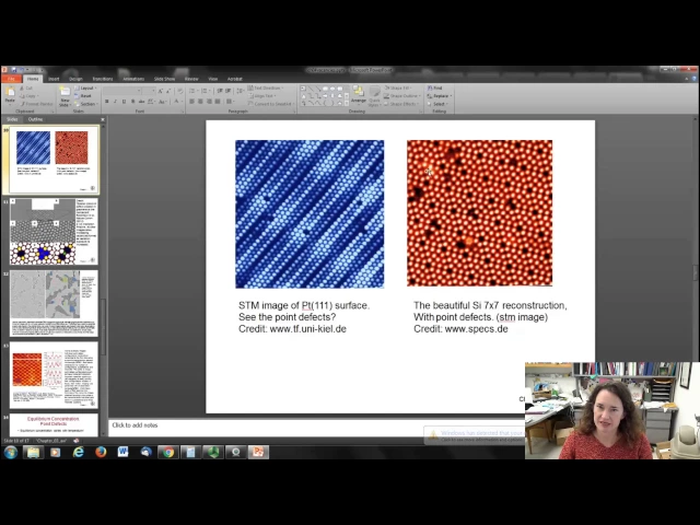
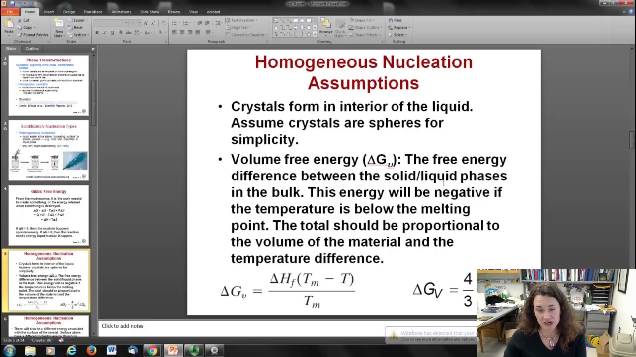
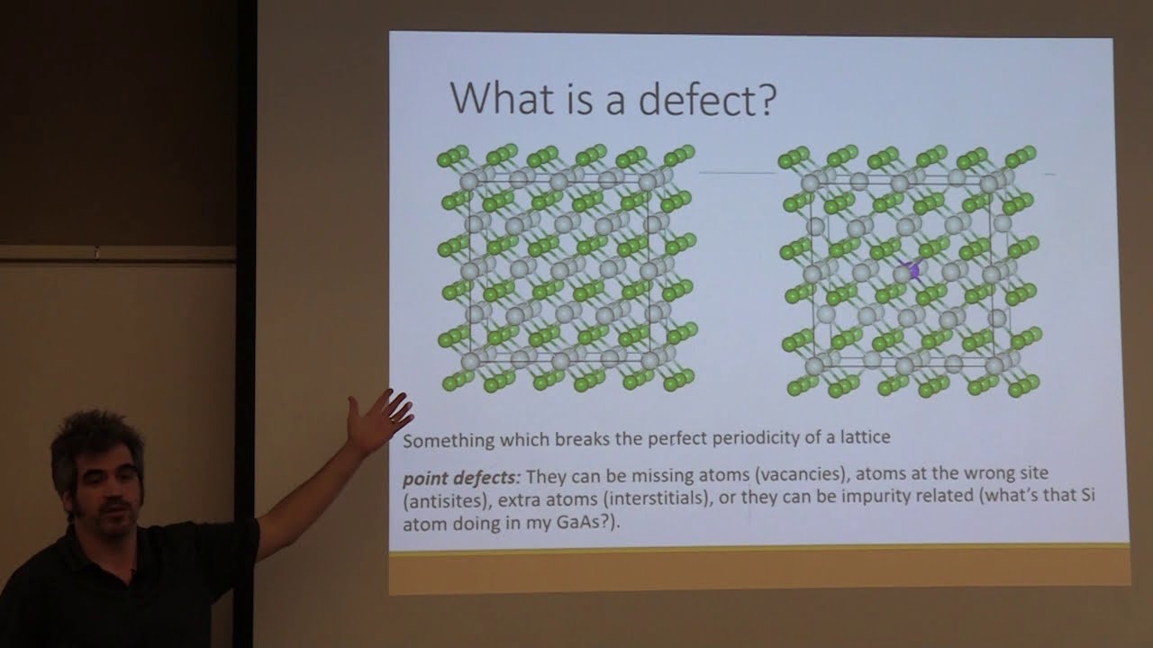
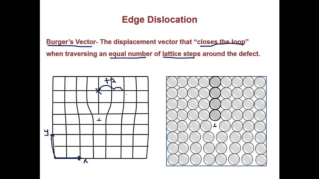
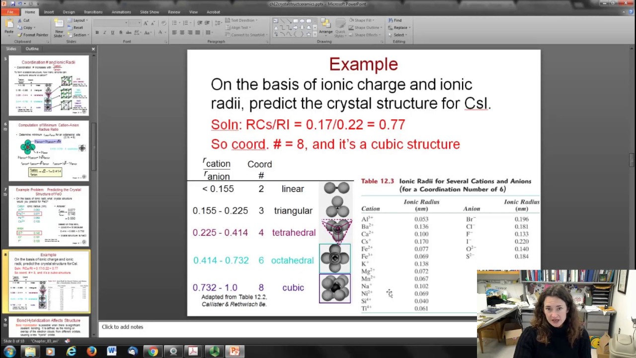
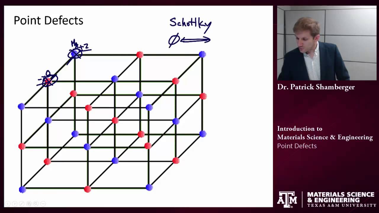
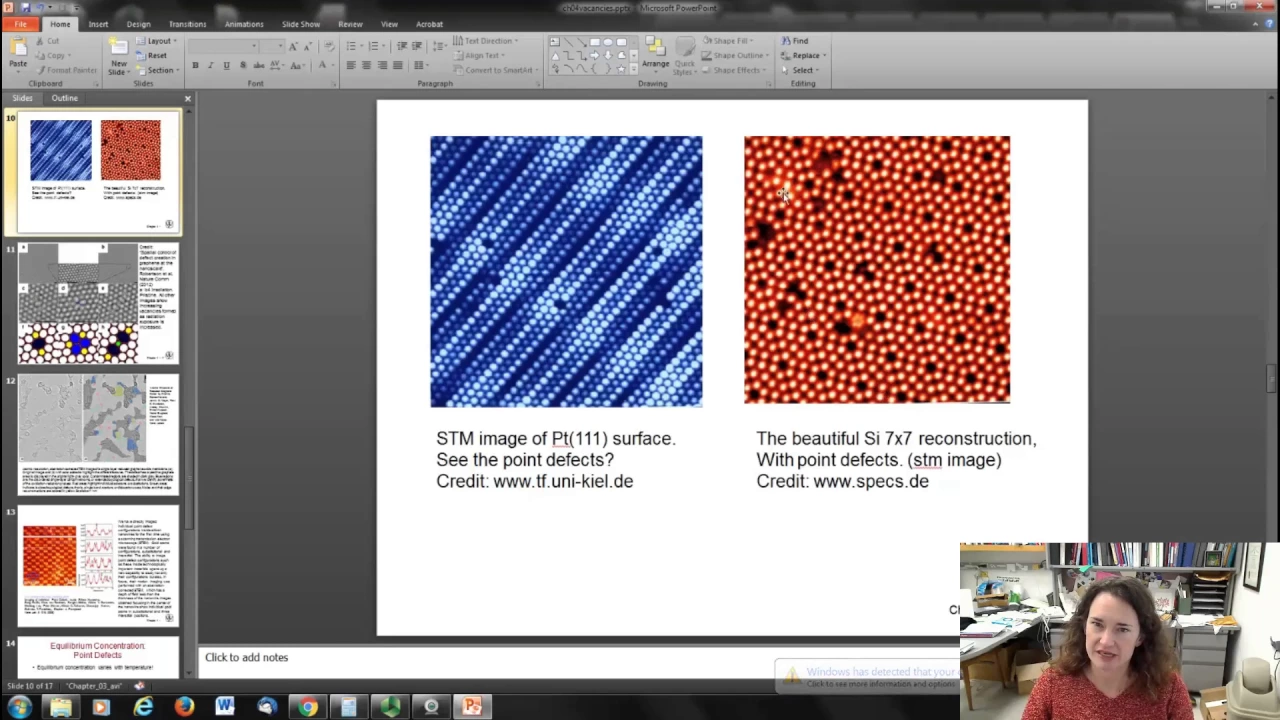
hi so we're going to start a new chapter in chapter 4 and it's on defects or imperfections and solids so in this chapter we're going to cover the ideas of how defects are formed when a material solidifies what kinds of defects are there in solids can you control the number of types of defects how these defects affect the material properties and are they even undesirable or are they something that we would actually want to happen sometimes so in chapter 3 in all those previous lectures we really just sort of assumed that the order in a crystalline structure was absolutely perfect and there were no defects or irregularities but real materials of course are packed full of defects and lattice irregularities and they have many many errors imperfections that have dimensions on the order of an atomic diameter too many lattice sites so we can classify defects according to their type of for geometry their point defects line defect Lane defects and we can also classify them according to how big they are the dimensions of the defect one place that defects or imperfections can arise are when a material actually solidifies when it becomes a solid from the liquid state so for example let's say that you're casting a molten metal okay so when that happens you start off with a liquid material and then what's going to happen is inside the materials they'll be see these little nuclei or seed crystals that start the solidification process now where these form could just see from random thermal fluctuations for example you have atoms kind of just moving around inside the liquid and at a certain point just due to statistical fluctuations you get a high density region and that's all it takes to get the process started or it could come from impurities inside the molten material itself if there's some irregularity something inside there that's already solid some sort of defect in your liquid then that can form as a nucleate nucleation point as well but however it happens you had these little nucleation points throughout the material and then the crystals start to grow words from these nucleation sites so you have solid regions that are growing outward inside this molten material now eventually they're going to meet up with another region with a neighboring nuclei that's been growing outward now they might not have been perfectly oriented with respect to one another when they form in fact it's most likely that they weren't that this one over here had a crystalline orientation that was tilted this way and this one tilted this way and then eventually when they meet up you're going to have a boundary where the crystalline structure isn't the same when they meet up and so that leads to what's called a grain structure and a material and so you have these grains your domains where the crystalline structure is the same within the domain but although it might still be you know FCC lattice or whatever it's rotated with respect to the neighboring grain and so you're going to have defects present at those boundaries so you have planar defects that arise when dissimilar crystals meet so that's one source of defects if you zoom in at these grain boundaries and you're gonna have these angles of misalignment and you can see that where the crystalline boundaries meet up then you've got a lower density right there well that lower density means that in between crystalline grains the atoms have higher mobility it's easier to move around when the density is a little bit lower because it's easier to move around they're going to diffuse easier crystalline boundaries and also because they're not quite as tightly bound to the atoms at a boundary these atoms right here at Crystal and grain or not as tightly bound then they're going to be more chemically reactive it's going to be easier to get them to chemically react because they're not as tightly bound energetically as their neighbors so there's a lot of things that can happen at grain boundaries for that reason so here's an example of a TR an SEM image of some grains that are shown here now you can have grains that have kind of a structure um where they're columnar or elongated or they grow in certain directions or can they can be homogeneous or eques acts and they're rough the same in all directions here we see one that definitely elongated along a column and what happened here with heat was kind of flowing outward in a certain geometry and that caused the crystals to grow along that axis preferentially and so you have this really pretty interesting structure that resulted from that sort of non-equilibrium cooling now even without this scenario of the crystalline grain boundaries there's still no such thing as the perfect crystal okay you could have the slowest cooling in the world and have a perfectly homogeneous defect free crystals with no boundaries and you still have defects within your crystal for one thing you can have vacancies vacancies are when a lattice site within a crystalline structure just isn't occupied and those are unavoidable because of thermodynamics basically the entropy just can't be minimized to the point where you don't get these vacancies often however these vacancies actually help you out or the defects help you out for example in an alloy a blend of material properties actually improves the material mechanically in many cases it's desirable you can also strengthen or harden material by decreasing the grain size going through something called strain hardening and of course if you decrease your grain size you've got more grain she's got more boundaries you've got more defects but that changes the material properties oftentimes in a desirable way so lots of times defects or your friend if you want a stronger tougher material so going over the types of defects or imperfections that you might see you have vacancies we are to kind of talk about that that's when an atom site lattice ID is not occupied by an atom you have interstitial atoms and that's when you have atoms that are kind of worming their way into something that's really not a lattice site and then you have substitutional atoms and that's when for example let's say you're making copper you might get a little bit of nickel in there too so that's a substitutional a nickel atom will occupy a lot of site that of copper atoms should be in so that's a substitutional defect you can also get dislocations which are lined defect and grain boundaries which are area defects and we'll talk more about those in the next lecture so point defects vacancies basically you've got these vacant atomic sites on a structure and what that causes is it causes a strain in the lattice okay the neighboring atoms are going to want to go inward to sort of compensate for that vacancy okay so that causes this distortion of the plane you can also get self interstitials so that's when you have say this is a copper lattice for example you have a copper atom that kind of worming its way in where it's really not wanted there's not really a lot of site there but it kind of gets stuck there okay and that causes a tension in the lattice as well it causes this the lattice lines to vote outwards like I've shown here this so those are extra atoms so here's a picture that shows a whole bunch of different kinds of possible point defects there's a self interstitial you can see it's kind of crowded in there there's a vacancy and we already talked about now you can also have impurity atoms in there like I talked about with the nickel and the copper let's say that this is a nickel atom occupying the copper lattice site okay and you can get interstitial impurity atoms let's say for example that this where iron and this is a carbon atom right here a little carbon atom the midst of all this iron so it can fit into a smaller spot then an iron atom would occupy and it's an interstitial impurity on so the fun thing is that now with today's advanced microscopy we all just have to theoretically compute or model these things anymore we can actually image the defects point defects directly which is really really super awesome in my opinion so here are a couple of scanning tunneling microscope images of different metal surfaces so this is a platinum one one one surface and you can see the point defects and these are real images of the surface so here's some vacancy sites in there you can see they're easily not beautiful platinum one one one surface and this is the gorgeous silicon 7x7 reconstruction so silicon undergoes a phase change to higher temperatures to a different solids and you can see in here a number of different kinds of defects you can of course see the vacancies those are pretty obvious right away there's also some things going on with substitutional atoms you can see that there's something there that probably doesn't belong there all right and then you can see some self interstitials in this image as well I think there's one right here that you can see so there's defects that can be seen directly in scanning telling microscope images now the fun thing is that you can also take movies so if you want to you can take a series of STM images of a surface once you get your atomic structure and you can watch these defects move around make a little film so that's fun this is a transmission electron microscope image for transmission electron microscope fermions make sense sections and - - through these guys were actually controlling the number of defects and graphing at the nanoscale by radiating it with the electron beam so they took a quick picture and you can see this beautiful pristine image of the graphene and then they irradiated it for varying lengths of time and continued to take images at the surface and you can see that after they irradiated a little bit they created one vacancy they rated it more they created more and it changes the lattice structure as they show here in this cartoon down here as they irradiated more and create more vacancies and then here is an aberration corrected transmission electron microscope image of a single layer of graphene oxide and you can see here they've taken the raw image and then I've color-coded it to show the types of defects so blue regions are one kind of defect disordered single layer of carbon networks red areas or individual ad atoms or substitutions green areas or isolated topological defects like bond rotations or dislocation cores and holes and their ads are in yellow so you can see they they color-coded it for the type of defect which is kind of fun and then finally just one more because of course this is my thing in them super excited about it always been anyway this is a scanning transmission electron microscope image of some silicon nanowires what they show here is substitutional defects substitutional interstitial atoms so within this silicon nanowire you can see these little gold atoms that are cropping up where they're not supposed to be okay so that's kind of fun too all right I promise that's all now the equilibrium concentration is the number of point defects varies according to the temperature and so this is the relationship here here we have the number of vacancies divided by the total number of atomic sites so that's n V over N that creates a little fraction of the total number of defects in the sample so you have a fraction that's established there and it's got an exponential dependence so here we have either the minus QB over KT QV is the activation energy which is the amount of energy that it takes to create that vacancy in the first place to just launch the atom from its site okay and that's usually a fraction of an electron volt in energy K is Boltzmann's constant it's the sort of thermodynamic constant one point three eight times ten to minus twenty-three joules per Kelvin or eight point six to 10 7 minus 5 DB per Tilden pick your poison there and to get the temperature in Kelvin okay so that's the formula dictating the number of concentration number of concentration of defects and we can get the activation energy from an experiment for example if you have a material and you vary the temperature of that material and measure the number of defects with a fraction of defects and you can get an exponential dependence so here as we increase the temperature we see this exponential curve forming right here and then you can take the log of both sides and that forms a straight line and from the slope you can extract that activation energy okay so if you want to do that you can so the example that I'd like to show here is for estimating vacancy concentration so this one says final fraction of sites that are vacancies in a lab at 327 Celsius which is 600 Kelvin the Gibbons are the density of leads 11. 35 grams per cubic centimeter the atomic weight of lead which is 207 two grams per mole the activation energy for creating a vacancy which is 0. 55 electron volts per vacancy created and then of course Avogadro's number 6.
022 times 10 to the 23rd atoms per mole to this our Givens we're going to use our formula and say that the fraction of fraction of vacancies is equal to the number of vacancies divided by the total number of bytes and B over N and then that's equal to e to the minus QB over KT so if you plug in for QB you get e to the minus 0. 55 e V divided by Boltzmann constant eight point six two times to the minus five times the temperature and then you get the fraction is two point four one times ten to the minus five all right now in one cubic centimeter of the material how many defects would this correspond to okay so in order to get the number of defects you multiply your fraction times the total number of atoms in the lab so here the total number of atoms in the lattice would be the fraction two point four one times ten to the minus five times and Avogadro's number 6.