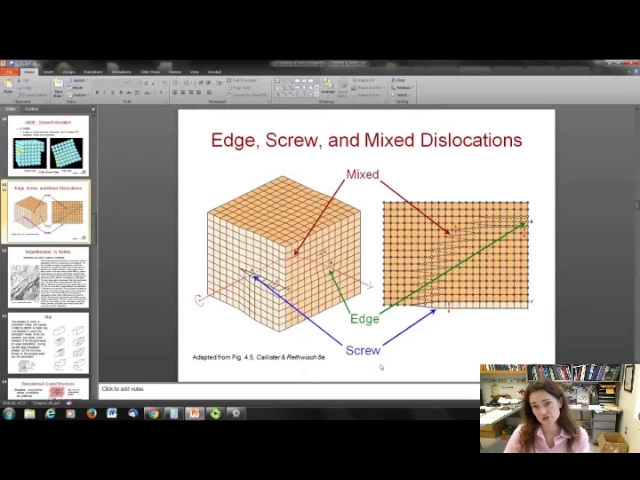
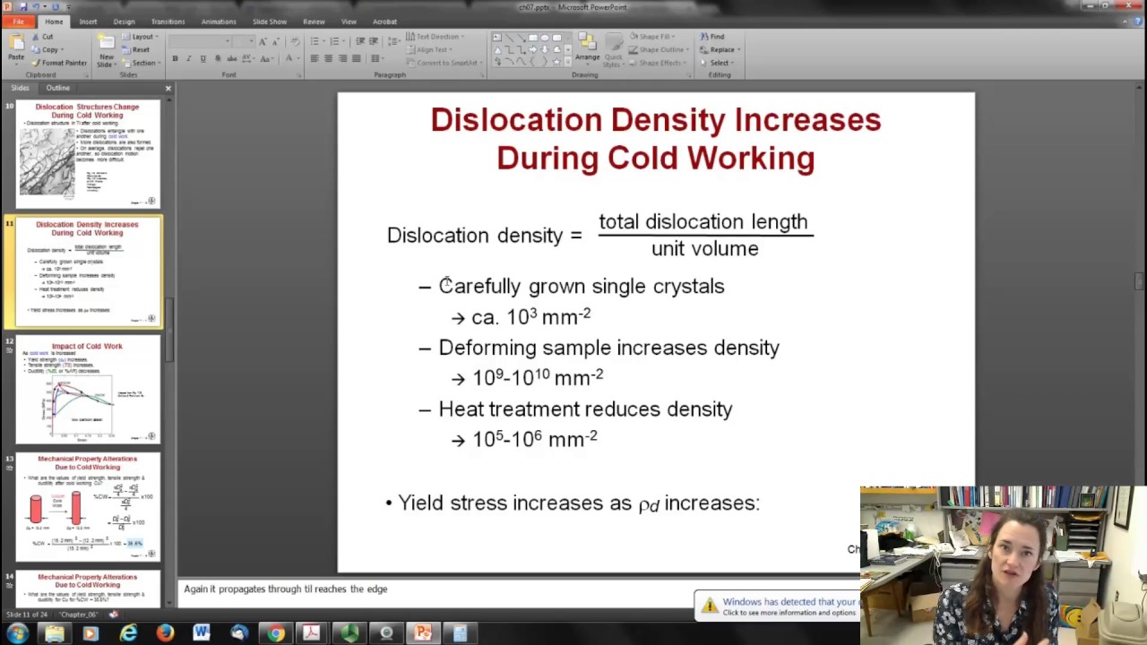
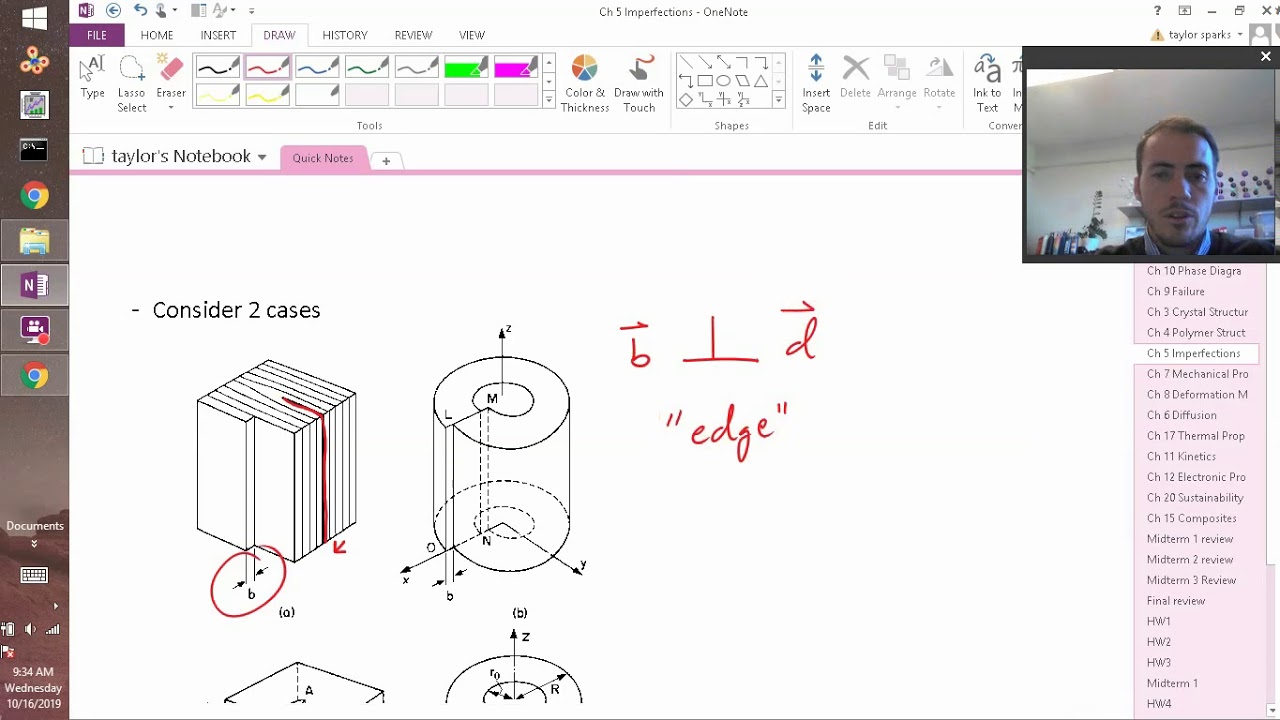
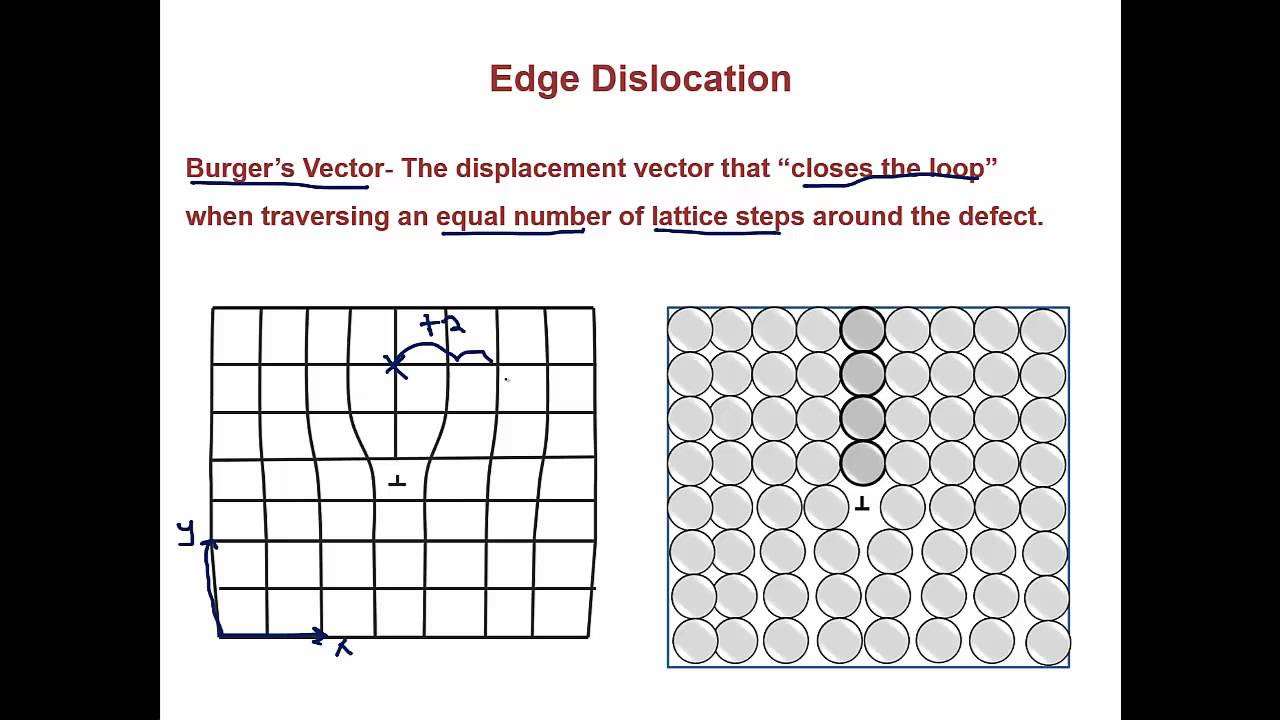
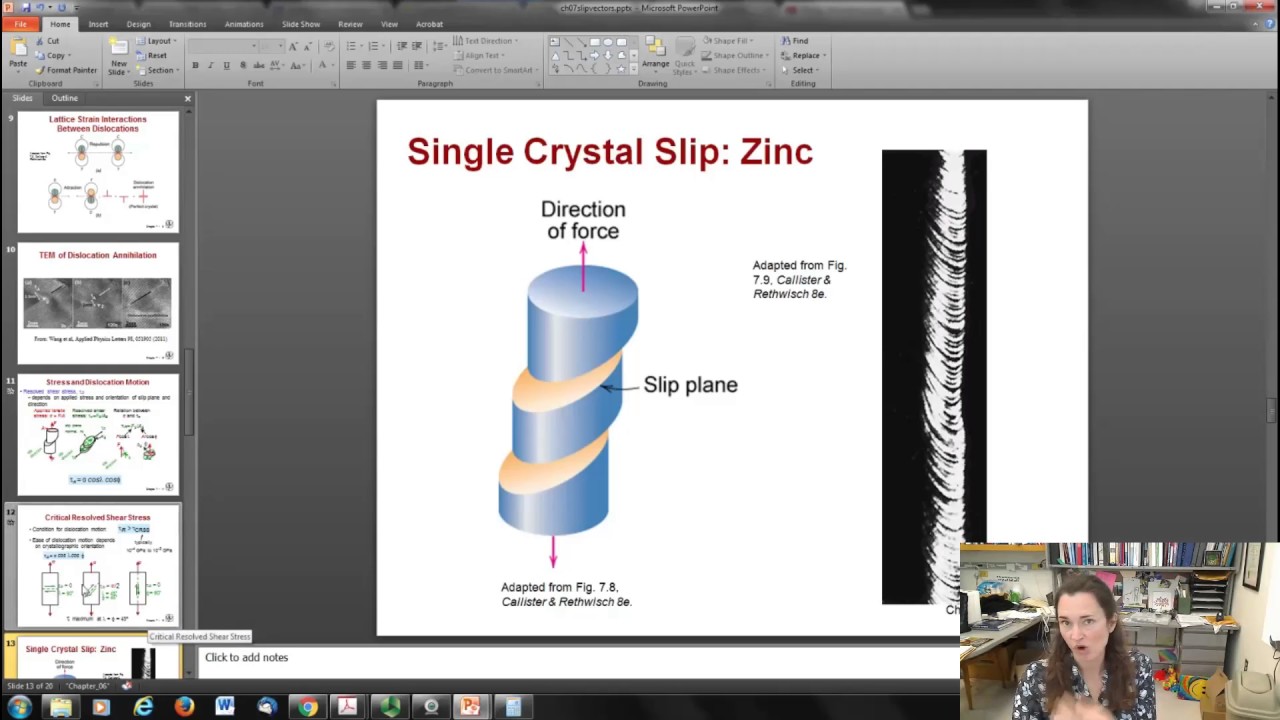
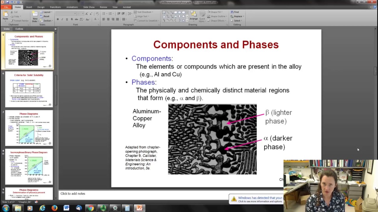
okay um I'd like to now speak about line defects plane defects and microscopy to finish off chapter four um from your material science textbook so first line defects or a u basically a one-dimensional defect are dislocations they're called dislocations and what happens is slip between Crystal planes actually results when dislocations move so you have a line defect it's moving along this dislocation is moving along and this causes um or produces permanent plastic deformation so there's two kinds of deformation when something is deformed it can deform plastically which means it's permanently deformed kind of like smooshing a piece of silly putty or plastic or it can deform elastically in other words you stretch over rubber man and it bounces right back so plastic deoration is permanently altering the material so for example um if you look at this zinc um hexagonal close pack lattice and you deform it then what'll happen is it'll stretch out and then when it stretches out the uh relaxation of the lattice happens along very specific slip directions um and it causes really cool looking effects that are pictured in your textbook now um we we talk about the burgers vector and uh linear defects um in terms of the Burger's Vector so basically if you have a one-dimensional def um then that can be when the atoms are misaligned and that can be the beginning of your slip plane so the burgers Vector which is often abbreviated um with a lowercase b it is a vector so it has a direction and it's named after the Dutch physicist yon Berger um and the magnitude and the direction is best understood from this little graphic that you see here so this perfect lattice right here um you can see makes this perfect little rectangle but now if we introduce a defect here um which is symbolized sometimes with that little perpendicular insert for an edge dislocation is symbolized by that little T um then what happens is it stretches your rectangle out it distorts your rectangle now the direction and the magnitude of the Distortion of the rectangle will give you the Burger's Vector so here because your rectangle is basically opened up in this direction the burgers Vector points along that and connects um the original rectangle to the new stretched out rectangle so it kind of completes it in in other words if you have to splice a new little wire in to finish out your rectangle the Burger's Vector would be the slice now that's for an edge dislocation down here we show a screw dislocation which is basically taking the planes and shearing them this way and introducing a defect there um it's a little more threedimensional than two-dimensional so you can see here you have this perfect little rectangle and then what happens is the rectangle gets torqued like that okay when the rectangle gets torqued like that then the burgers Vector um which completes that rectangle uh connects the rectangle that's opened in this direction so the burgers Vector points perpendicular to the plane um uh of the atoms the original atoms okay so in dislocation the burgers vector and the dislocation line are actually at right angles to one another but in screw dislocations they're parallel if that makes sense okay so here's uh an example of an edge dislocation and that's basically when you have an extra half plane of atoms inserted into a crystalline structure so you have extra atoms inserted in the dislocation line is parallel to that extra half plane of atoms and then the burgers Vector is perpendicular so the extra half plane of atoms run this way in that diagram and the Burger's Vector points that way so they're perpendicular to one another okay hopefully that's uh that's clear and that's why Edge dislocations are often symbolized with a little symbol that we use for perpendicular okay here's a um an image a temem image of an edge dislocation so you can see I'm not making this up um this was taken uh from a lead um toride sample here and then an antimony toride sample below and you can see that there there's a lattice mismatch there um and that causes that extra line of atoms to go along and because the lattice mismatch is very regular if you looked at a zoomed out photo you can see that the extra um extra line gets inserted in a regularly spaced fashion across the whole image now what happens is if you place your material under some kind of stress you apply a force to it and then that force is spread out over the area of the material producing a stress then what happens is your Edge dislocation can actually move or migrate under that stress okay so for example in this um cartoon here what's happened is you have a crystall in lattice and it's being sheared so the top is being pushed one way and the bottom is being pushed another and that introduces that stress and that causes the plane of atoms that is that dislocation to hop along and move through so it it actually moves through like that there's a movie depicting that in a two-dimensional way here let me show that movie and you can also go back to the uh slides on your own and see how they move around and hop and they do that actually to minimize their energy so what happens is when the force is applied that adds a little bit of energy to the system enabling the atoms to move to a more energetically favorable configuration I'll play the movie one more time and you can see them kind of H hopping along in the dislocation moving through okay so what's required for that to happen is bonds across the slipping planes are then broken and then reformed with new atoms in succession as it moves across okay so for screw dislocations what happens is if you they're called screw screw dislocation because if you had a succession of them all in a row of course it would form a screw um and that is a planer ramp that results from a sheer deformation and there we have our Burgers Vector parallel to the dislocation line so in other words the dislocation causes that plane of atoms to pull out of the cube and because you would have to draw a line since your rectangle shears this way the burger spectr will point in the same direction um that the dislocation is okay so it's parallel well um if you're confused about what these things might look like in three dimensions there's some um apps available to you through your textbook hopefully you can still access that even though you purchased it used but if not you can Google them and then that will enable you to do a three-dimensional rotation of the crystal so that you can see what the different dislocations look like to um all sides from all sides and you can even see the animations if you want to do that so that's kind of fun I encourage you to do that now it's not like you just have Edge dislocations or screw dislocations you can also have any combination of the two um in a real material um that's depicted here in this cartoon so you can have Edge dislocations screw dislocations and mix dislocations I'm not making this up you can actually see these dislocations um in electron micrographs so in order to do this um you have to make a really thin section of your metal and stick it in a transmission electron microscope and then they'll pop out as darker spots on your image and the reason for that is that as the electrons move through the Crystal and lce of course they're defract it a little bit and they defract one way through a perfect lattice and then they defract in a slightly different angle when they hit a dislocation because the density is different for the atoms at dislocations um and because the density is different and they're defract in a different direction that makes the dislocations themselves appear dark or shadowed um and so you can see that in a temem they appear these dislocations appear um at magnifications from anywhere from 50,000 to 300,000 times now if you know anything about electron microscopy you might be saying to yourself well I don't need a tem to see something like that uh scanning electron microscope is plenty good um enough to see that magnification and that's true but in order to see the dislocations you generally have to shoot the electrons through the material and that's why T is required even even though the magnification is relatively low um compared to what temm can do in millions of magnification okay now we've discussed dislocations but the process by which a dislocation actually moves and causes the material to permanently plastically deform is called slip okay this is called slip so the direction that the dislocation moves in is ter is termed the SL slip Direction and the slip direction will be in the direction of the burgers Vector um for Edge dislocations so drink slip The Edge dislocation actually uh sweeps out a slip plane that's formed by the burgers vector and the dislocation for Edge dislocations okay so because the um the burgers Vector is perpendicular um for Edge dislocations that sweeps out a plane okay now when it comes to the slip Direction um you might be thinking well which way does it go generally um what happens is that the close pack directions and planes are preferred for slip um and this makes sense because along a Clos pack Direction you have more atoms per unit length and then um it means that it's less distance for each of those little atoms to hop if you picture the movie if there was a longer distance between those um lce sites then it would have to hop further so it makes difference makes sense that the close pack direction would be the preferred direction for the slip um and that leads to the smallest expenditure of energy so as an example we can calculate the length of the Burger's Vector in Copper okay so if you look up what the um lattice structure of Co copper is it's an FCC or a face centered cubic um lce now the um the direction with the closest packing in FCC is along one of the diagonals of the faces okay now of course the family of directions would be the same um it would be close packed along any of those diagonals of the faces that's the tightest um this dictates a family of directions the family of direction is indicated by these sort of triangular looking brackets greater than less than brackets here that's a family of Direction so we're gonna call the Family the 110 Direction um to uh as depicted in this little cartoon here across the bottom that's the close packed Direction so that's the direction now the um length of the vector the length of the Burger's Vector would be the shortest hopping distance across that Clos pack Direction um so in other words if the atom were to hop it would have to hop from this top left corner to the Center for example and that is going to be that distance is going to be two times the radius of your atom so for copper the atomic radius is1 128 um so double that and you have a length for your Burgers Vector of 0. 256 and then so the length is 0. 256 and the direction is 110 and that specifies your Burger's Vector okay now slip and slippage in metals help explain why the strength of metals is so much lower than the value that you might guess looking at the strength of the metallic bonds so for example if you had to break an iron bar and you had to break all the bonds along the whole cross-section in order to do that you'd never be able to break the bond because you'd have to exert a force of several million pounds per square inch to get that to happen but instead what happens is you deform the bar by causing slip and then only a tiny fraction of those bonds actually have to be broken to break the bar and that allows you to use a force of like 10,000 pounds per square inch um in order to to break the bar um that's also the reason that Metals um in general have a tendency to be more ductile because they have these easy to deform slip planes and that allows you to stretch them out um and form them into wires to prove to you that I'm not making this up these are some images of some fractured um surfaces so these surfaces have been fractured and you can see that the cracking actually started along these grain boundaries so here um the length scale the scale bar there is 25 microns 20 microns so these are the grains and you can see that the fracture started along the boundaries of these gr grains um and of course a green boundary is a defect so it's easy for slip to start at the defect site this is just sort of fun to think about if you think about the density of dislocations or the slips then the length this is the length of the dislocation per unit volume so if you went think back to that picture that we had the temm cross-section um showing the little lines so this would be the total length of all those little lines per unit volume of your material for the softest Metals this is about a million centimeters per cubic centimeter um and it can have densities of up to 10 12 cm per cubic centimeter um if you deform the material so most metal are absolutely packed with dislocations and line defects you can also have planer defects or so-called interfacial defects and these occur at boundaries um so for example I don't know if you've ever thought about this but the outside of a metal is actually one great big defect because there's no Metals touching it no metal atoms touching it on the other side so the surface is actually considered a defect in Material Science um so external surfaces grain boundaries are also considered defects because the lattice doesn't match up there um phase boundaries things like that um domain walls and furom magnetic materials these are all different kinds of defects that are basically planer defects and not line defects so you can have planer defects or grain boundaries caused by a series of um Edge dislocations you can see here we have a crystallin orientation of One Direction on one side and a crystalline orientation of another on the other side and that causes this grain boundary that has crystalline orientations that are different by that specified angle okay and that's because of the series of edge dislocations you can also see that here so this is a another um electron micrograph showing these two materials meeting up in the angle of misalignment so what's happening here is at the top you have nickel and silicon alloy and then here the bottom you just have silicon and what that causes is these series of edge dislocations that causes an angle of uh uh to form here at the boundary because of a misit of about 15% so that's pictured there in that um electron micrograph um planer defects defects of course have um higher chemical reactivities which means that um for things like a catalyst a catalyst is a material that increases the rate of a chemical reaction without actually being consumed itself so you add Catalyst to speed up chemical reactions um catalysts active sites at catalysts are often at um grain boundaries or defects um so normally they're surface defects and this is because the atoms of the defects are in a higher energy State than the interior atoms and that makes them more volatile so here in the image you can see um single crystals that are used in automotive catalytic converters um to get the uh to get the cars to run all better and everything and you can see here that there's all kinds of edges and defects um and often they increase the surface area to volume ratio of a catalyst just to increase the number of defects because of course a boundary or the edge is a def is considered a defect and that increases the reactivity of your um material this is also another reason that nanop particles are um such good catalysts are more chemically reactive because their surface area to volume ratio is a lot larger than macroscale materials so they have more defects okay um microscopy is used a lot in Material Science um for analysis of materials to figure out their structure and their morphology and how the processing um is impacted by the morphology so uh we did a little little experiment the other day um in class where we had a um two-dimensional Crystal grown and an image between two cross polarizers and you can see the grain boundaries so that's very similar to what's pictured here there's a um there's an a iron chromium alloy here and you can see the grain boundaries in the image so here the grain boundaries are considered imperfections and they're more susceptible to etching um so what they did to prepare this sample instead of having a um section that's transparent to light and putting it between two cross polarizers what they did was they etched the sample a little bit um and that allowed the um grain boundaries to be uh revealed that way and then they stuck in under an optical microscope and they saw the dark lines corresponding to the grain boundaries um now there's a lot of standards in Material Science these standards exist for the safety of the public so the ASM stands for the American Society of test in materials ASM and this um body has established industry standards um for different things so if you're going to say this material is rated for use for this application then what that means is that it's had to pass a lot of quality checks along the way um we're going to learn more about the different quality checks that materials might go through as we go through the course but one of those things that might be considered a quality check includes what is the grain size for the material that you're looking at so one of the ASM standards that's um set out is to give the ASM grain size number so that's Quantified via this little equation right here what you do is you take an image of your material at 100 times magnification in an optical microscope and then you display it at 100 times magnification and then you count the number of grains per square inch in your material at that 100x magnification okay and then that equation here big n is the number of grains um per square inch the 100x magnification and that's equal to two to the power of little n minus one and little in here is the ASM grain size number okay so in an example problem from your textbook this is number 34 in the version eight of the tech material science textbook if you have an ASM grain size of eight approximately how many grains would there be per square inch and a magnification of 100x and then also how many grains per square inch would there be without any magnification in the real material in other words in the cross-section of the real material so to solve this we're going to use that little equation Big N is equal to 2 to the^ of little n minus one if little n is 8 then that means Big N is equal to 2 to the 7th power and 2 the 7th power is 128 grains per square inch that would appear in that image at the magnification of 100 now if you remember um you've probably heard this before hopefully I'm not telling you anything you hadn't already heard but the magnification as defined for a microscope is equal to in one dimension the displayed length over the actual length so if you say that you are looking at something at 100 magnification and at a 100 magnification it's one inch in that Dimension then that means it's actual di menion on the sample is 0.
01 in okay so you're really looking at at that size 0. 01 Square 0. 01 inches quantity squared without any magnification now that means that your your image is a factor of 10,000 magnified or or larger than your actual so you would have to multiply by a factor of 10,000 to find the actual number of grains per square inch with no modification and that would give you 1.
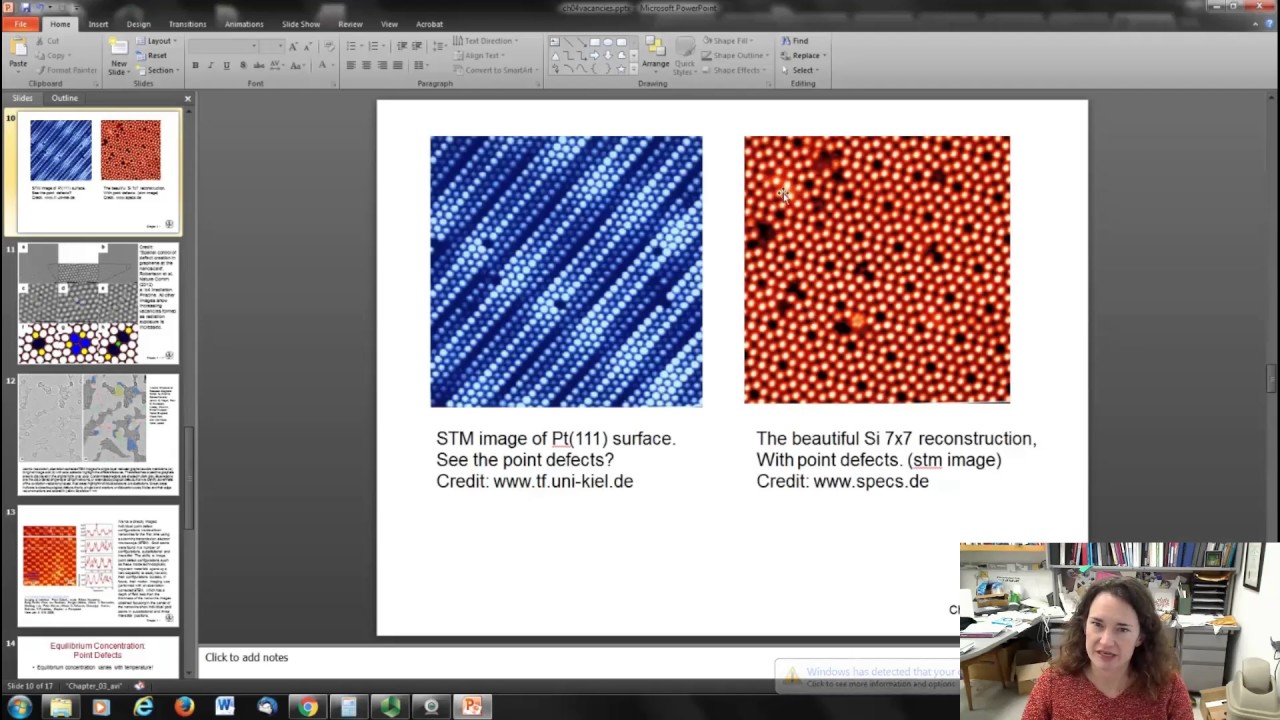
28 * 10 6 grain per square inch on the actual sample hopefully I didn't garble that too much and it makes sense now there's a number of different microscopies out there um and each one of those microscopies is good for a particular job and at a particular length scale okay Optical microscopy isn't going to solve all your problems neither is electron microscopy you have to find the right tool for the right job so there's different kinds of microscopes out there on the market now of course there's your your eye that's one way of viewing a sample um and that's good from about say 10 to the 5ifth nanometers up you can see things um and then if you use an optical microscope typical Optical microscopes can magnify things say up to a thousand times um and so that gives you a size scale of about um something times 10 the 2 nmet you're going to be limited by the wavelength of light basically Optical microscope aren't going to be able to do better than that um and the wavelength of visible light begins at 400 nmet so that's kind of your ultimate resolution for an optical microscope and then that goes up from there um scanning electron microscopes this is where you have a beam of electrons um that is then focused down to a spot and then what happens um is you scan the spot across the sample um and uh that forms an array a two-dimensional array of data points and the brightness of each pixel in that image corresponds to the signal that you get out created by that Electron Beam that could be the back scattered electrons the secondary electrons the x-rays anything that's created by that Electron Beam um can be used as a signal um and then different types of images displayed so that's kind of scanning electron microscopy in a nutshell scanning electron microscopy's resolution is therefore going to be limited by the size of the spot that you can create on your sample surface so that's going to be at best on the order of a few nanometers um so that explains the lower limit on the Range on scanning electron microscopy images transmission electron microscopes though there you have a thin section of material and you shoot the electrons through so transmission electron microscopes you're not creating a spot so that doesn't limit your resolution what limits your resolution in aberration corrected transmission electron microscopes is the wavelength of the electron itself as dictated by planks constant um divided by the momentum so remember for matter waves Lambda is equal to H over P where pure momentum transmission electron microscopes are actually limited um when their aberration corrected to the wavelength of the electron so that's gives you very very low subatomic at times resolution and then finally scanning probe microscopes um there's a couple of different kinds of those um scanning tunneling microscopes scanning um scanning Atomic Force microscopes these are two different kinds of scanning probe microscopes and those are going to be limited in part by the radius of your probe um so it's just how sharp can you make your tip um and then sometimes you can get to some fraction of the radius of your tip they're getting good good tip radi these days and they've actually gotten um tip Radia on the end or the sharpness of some of the STM tips down to a single atom um which means that you can get subatomic resolution in the skin probe microscopes as well so that's pretty um impressive so that's your sort of in a nutshell what's going on please do read those sections of your textbook and if you find microscopy particularly interesting we do have a microscopy course um that uh covers this so I encourage you to take that one fun thing about scanning telling microscopy is that the atoms can be arranged um an image you can apply a field and kind of pick an atom up and move it to a new location you might have seen the little cartoon that's out there now it's the smallest cartoon in the world where they had these atoms that they moved around on a Surface um in a succession of images and then made a movie out of it um it was it's really cute if you haven't seen it um do check it out and then if you have an aberration corrected transmission electron microscope then you can get you know true subatomic resolution um they're really fantastic things the closest one of these to us we don't have one of these on campus we have a transmission electron microscope but not an aberration corrected one um the closest one of these are probably in oid oid National Labs or University of Tennessee Knoxville they have some there um aberration corrected just means that you know in an ideal Optical system all the Rays of light from a point on the object plane would converge to the same point and that forms a clear image but of course that that never really happens so you have to correct for these defects um for a long time it was very difficult to do that with an electron microscope but to a certain degree now they have actually overcome those difficulties um and you can get resolution down to less than 0.