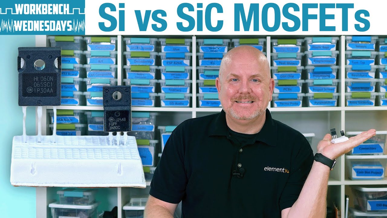
in 2018 tesla inverted our expectations and shook the ev industry when they adopted an st micro electronic silicon carbide based inverter for their new model 3 electric vehicle it allowed tesla to shrink one of an ev's most critical components in half and it has sparked new interest in a silicon technology as old as the industry itself in this video we're going to take a look at the powerful benefits of silicon carbide based power electronics but first the asian arbitrary newsletter check out this newsletter about america's largest semiconductor equipment company applied materials it felt like it
was a pretty in-depth write-up the sign up link is in the video description below i try to put one out every week maybe two alright back to the show silicon carbide exists in meteorites but almost nowhere else naturally almost all of the silicon carbide in the world is synthetically made it is a really beautiful rock though i love rocks edward goodrich atchison an assistant to thomas edison first produced it in industrial quantities all the way back in 1890 while looking for a way to make artificial diamonds he heated silica rock and powdered carbon called coke
up to 2600 degrees celsius in an electric furnace this resulted in coarse grains of silicon carbide his method is still used today in industry the atchison method made up of equal parts silicon and carbon there are over 200 known crystal polytypes variants in the silicon carbide multiverse it is not fully understood why there are so many poly types but they all have their own unique physical traits but only three can be used for electron devices 3c 4h and 6h 3c wafers are not commercially available due to instability at high temperatures so practically our choices are
just 4-h and 6-h while people have studied the 6-h variant most commercial research is consolidating to 4-h silicon carbide is extremely hard it was the hardest synthetic substance known to man until the creation of boron carbide in 1929 in industry they use it in body armor to grind things down and as the abrasive for sandpaper but when it comes to electronics silicon carbide has a special feature that allows as transistors to operate at both higher voltages frequencies and temperatures than traditional silicon silicon carbide along with other materials like synthetic diamond and gallium nitride are referred
to as wide band gap materials what does that mean semiconductor materials have something called a valance band and a conduction band when electrons get too much energy and get too excited like from a high dose of thermal energy they break into the conduction band when the electron gets into the conduction band they are like little free agents capable of carrying a charge somewhere referred to as charge carriers furthermore when the electrons broke out of the valance band they leave behind positively charged holes remember electrons are negatively charged and those are also charge carriers capable of
doing conduction transistors work because they can assume either an on and off position roughly speaking when their electrons are in the conduction band the transistors become like internet commenters and cannot switch off becoming useless the band gap represents the amount of energy needed to make electrons jump out of the valence band and into that conduction band a buffer zone between control and out of control the wider the buffer zone the more energy needed to jump the bands silicon carbide not only has a super wide band gap but it is also an excellent conductor of heat
three times better than traditional silicon and second really only to diamond this conductivity makes it easier to extract and dissipate heat from any such device not a bad perk commercial silicon semiconductors thus top out at about 175 degrees celsius before they break out of their band gaps silicon carbide on the other hand can go up to 300 degrees celsius and beyond maybe even 900 degrees with the right packaging this wide band gap has applications beyond just heat resistivity as the voltage in a power device increases their electric fields get stronger as well when the field
gets powerful enough the device suffers what is called an avalanche effect the atoms break down and release large numbers of free charge carriers leading to very large currents moving through materials similar to the temperature situation silicon carbide's critical electric field limit before this avalanche effect breaks out is 8 to 10 times higher than that of traditional silicon that means a silicon carbide device can handle voltages as many times higher than silicon now that we know about silicon carbide's special powers and why they exist we can now move on to an electric vehicle and how they
can use them every electric vehicle has power electronics along with the battery and the electric traction motor the power electronics are one of the big three technologies enabling today's practical electric vehicles power electronic systems help charge the battery and power the motor they are generally made up of four components but arguably the most important is the inverter electric current comes in two flavors alternating current or ac and direct current or dc ac will flow in one direction for a period and then reverse to the other direction for the rest of the period dc on the
other hand flows in one direction only the inverter turns dc power from the ev battery into ac power that the ev motor uses to operate smoothly this is called switching a circuit that performs the opposite direction from ac into dc is called a rectifier today many of these power electronics are silicon based the two most popular power switching devices are the insulated gate bipolar transistor or igbt and the power metal oxide semiconductor field effect transistor or mosfet silicon base mosfet are for low voltage lower power and high frequency applications they dominate the market for applications
below 600 volts silicon-based igbt devices are used for high voltage high power and low frequency applications they dominate the market for applications between 600 volts and 6.5 kilovolts most ev inverters before the model 3 use igbt transistors the issue is if you want to go beyond that 6.5 kilovolt limitation go beyond that and the electrical fields get powerful enough to make things challenging for traditional silicon power electronics yet today's modern power electronics face relentless market pressure to do more more more the success of ev drive technology heavily depends on how efficiently the power electronics can
switch power while reducing operating costs inefficiencies in the switching process lead to power loss which materializes excess heat and additional energy demand furthermore power electronic circuits are placed near jet turbines or car engines really harsh environments with temperatures ranging up to 225 degrees celsius or higher so even more heat because of silicon's inherent temperature limits these power electronics have to be designed with active or passive cooling systems but these systems air-cooled heat sinks direct contact liquid cooling liquid cold plates and so on are never as effective as we want them to be these cooling systems
are also heavy and add more cost to the whole system a heavier more energy-hungry ev cannot travel as far or fast as traditional cars reducing their overall competitiveness incremental research continues but this is where commercial silicon carbide based power transistors can revolutionize things remember because of its wider band gap silicon carbide based power electronics can operate at up to 10 times higher temperatures up to 10 times higher voltages and up to five times higher switching frequencies it is a disruptive technology as friend of the channel bane once said silicon-based power electronics merely adopted the heat
silicon carbide was born in it molded by it people have seen silicon carbide's vast potential in the power electronics space ever since power electronics first entered the market in the 1950s so why haven't we seen silicon carbide based power electronics in the market until very recently some people believe the car companies are hiding an engine that runs on pure water is there a silicon-based power electronics cabal conspiring to hide silicon carbide from the whole world the actual answer is rather mundane as is related to the material itself silicon carbide's various strengths also contribute to its
weaknesses producing enough high purity silicon carbide wafers is hard today silicon wafers are made by first creating a big silicon crystal the crystal is made through the chokroski method growing a big crystal by repeatedly dipping a seed into the molten silicon melt the method has successfully allowed us to create today's biggest wafers i talked about this in a previous video go check it out the trokrowski method does not work without the liquid silicon melt but silicon carbide solid form directly passes into the gaseous form without first turning into a liquid to use a chemistry phrase
it sublimes before it melts because of this there is no melt and so silicon carbide wafers cannot be made with our traditional silicon methods we need to grow our silicon carbide crystals from gas until the 1950s the only way to produce silicon carbide crystals was through the atchison method the one where you combine silica and coke into an arc furnace and let it burn this worked fine for making sandpaper but hardly met the purity requirements for electronic devices in 1954 jan anthony lily of philips electronics discovered the lili method you take a tube of porous
graphite and surround it with silicon carbide then you heat the tube to 2500 degrees celsius silicon carbide will diffuse its way to the inside of the tube and crystallize on its cooler parts lili's early method created randomly sized hexagon-shaped platelets of varying crystal polytypes it was a step forward but still not suitable for wafers so in 1978 two soviet scientists tairov and svetkov modified the lily process to fix its shortcomings it works largely the same way but with very careful control of the temperatures and pressures scientists can grow one large crystal of a single polytype
this modified lily method referred to as physical vapor transportation or pvt meant that people can grow bools of one pure silicon carbide polytype at a rate of a few millimeters an hour it's not perfect however companies are still working to make larger sized wafers 200 millimeters or so and defect rates aren't exactly where people want them getting the wafers made to standard is probably the biggest challenge with the process but it isn't the only one silicon carbide presents some other challenges in the semiconductor processing for instance you can only cut the wafers with synthetic diamonds
which adds to the overall cost another thing is that pure silicon carbide is an insulator so it needs to be doped to conduct electricity but diffusing the dopants into the silicon carbide requires very high temperatures necessitating other methods and so on this section stretched very long but i hope i gave a decent overall view of the difficulties of making silicon carbide transistors infineon introduced the first commercial silicon carbide based power device in 2001 a schottky diode with vast advantages over the traditional silicon variant the next major new commercialization was the silicon carbide mosfet the power
mosfet is widely used by the industry due to its fast switching speed and suitability for high voltage and high current applications silicon carbide mosfet chips were first commercialized in 2010 by a north carolina-based company called cree they recently renamed themselves to wolf speed in october 2021. other companies soon jumped into the space including st microelectronics rom infineon and micro semi the ev inverter market has since grown into a multi-billion dollar market at the same time improved manufacturing processes have brought down the cost of the new devices what used to cost seven hundred dollars per inverter
unit in 2013 has fallen to just about 450 dollars in 2020 driven by cost improvements in the transistors and diode components though there is still a price gap with traditional silicon devices that price gap has gotten substantially smaller but even with the price gap you can design and deploy an inverter with far less attached cooling systems though space cost and size savings really add up and people anticipate that silicon carbide mosfets will start challenging silicon igbts in their traditional market strongholds it's an exciting time for silicon carbide there are easily hundreds of papers on this
space i wish i can keep going but the video has to end sometime this is the second time this channel has featured silicon carbide chips the first time was in my follow up to the soviet venus video which mentioned the use of silicon carbide technologies to build probes capable of surviving venus's brutal heat while i was doing the video i did not really believe that silicon carbide technologies can actually get there but tesla adopting the model 3 and the growing ev market have attracted a lot of attention to the space and other industries are starting
to benefit for instance solar inverters convert the dc power coming from a photovoltaic solar panel into ac power that the utility is capable of using silicon carbide solar inverters have shown 20 cost reductions over silicon based competitors extremely relevant in such a competitive space that future is quite bright indeed practical silicon carbide manufacturing is less than a few decades old we are still exploring the limits of where this technology can go i'm excited to see what future applications might crop up in the future all right everyone that's it for tonight take care of yourselves out
there subscribe to the channel sign up for the newsletter and i'll see you guys next time