Hi,Welcome to module 38. In this module, what we are going to do is, we have tried together a lot of things. As a picture we had, what the controller is supposed to look like as a black box, we also had almost a gray box description of what the data path must be, and then we had this top level module itself.
So, let us look at the top level module for a little while. So, this is the top level module, the top level module has clock and reset and it has 3 inputs; input 1, input 2 and GO and output and done. So, one of the things that we have not talked about so far is, what is the size of these inputs, because I am supposed to be calculating GCD of numbers and numbers have width as in the number of bits required to represent the digital, the decimal value, we need to decide that So, one of the things that will assume is input 1, input 2 and output, we will assume that, they are all 8 bits values.
So, these three will assume our 8 bit, GO is a 1 bit value and done is a 1 bit value. So, the first thing we are going to do is, we are going to write a module description for the top level module and this is a… So, what is top level module needed was actually two different modules. So, one of the modules is the controller and one of the modules is the data path and what the top level module internal have is a set of things.
So, let us start the description. What we need is, we are going to instantiate a controller, we are going to instantiate a data path and we are going to connect all of them together with this interface description. And so right now, this is the top down view of what we are going to do and this gives us a small problem at a time to deal with.
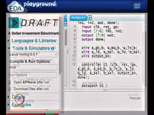
So, I am not worried about all the things that is going to go into the data path itself or how the controller is going to be return up, first going to write, what the overall systems is going to look like. So, this I am going to do as a Verilog module itself. So, let us see the design description for a GCD machine.
So, I am going to define a machine called GCD machine and the GCD machine is going to have several things. So, it is supposed to have clock reset and what not, so I am going to put all of those in So, I have clock and reset and I am going to have 3 inputs, input called go, an input called in 1 and another input called in 2 and we are going to have 2 outputs, one output called out and the output called done. And I have to specify, what each of these things are.
So, clock and reset are just inputs and the in 1… So, clock, reset and go are all single bit inputs. So, I will specify them as it is, in 1 and in 2 are again inputs, but I am going to specify them as 8 bit values, then there is output out and there is also an output called done. So, done is a single bit output and the actual output it could be a 8 bit output.
So, if I give the same number which are both 8 bit numbers, then I may get the result which is of 8 bit number, so I have that. So, this takes care of the module interface that we need for the GCD machine. Now, let us go back and look at the picture for the internal diagram.
So, the internal diagram says, the controller should be connected to the data path, there are a few signals that are going back and fore between the controller and the datapath. The input of the GO, the input GO of the design should go to the controller, the input, then there is clock and reset, which is supposed to go to both the controller and the data path And the output is supposed to come from the datapath, done is supposed to come from the controller, all these little things that we needed. So, let this is the slightly more detail picture of what we needed.
What I am going to do is, I am going to take this picture and I am going to write Verilog description based on this. So, what I already have is, a boundary view of what the top most design module is supposed to have, now I am going to look at the internals. So, the clock that is coming from the external world, reset that is coming from the external world, GO that is coming from the external world and so on, should all go to the controller.
So, these are the 3 inputs that will go to the controller. Then, there are three more inputs, namely a greater than b, a equal to b and a less than b, which will also come in to the controller; that is going to come from the data path and these four should go out of the data path. So, if I imagine this as I am going to buy 2 chips, one called controller, one called data path, I will still need wires to connect all of them.
So, let us look at all the wires that are needed. So, controller will need four wires, a select, b select, a load, b load to connect to the data path. Then, we will need four more wires namely a greater than b, a equal to b, a less than b and output enable, so will need eight wires so far to take care of various connections between the controller and the data path.
So, let us do those declarations first. So, what are the different things that we need? So, I will have a wire for a greater than b, a equal to b and a less than b.
So, I have three wires for that, then I will need four wires that are going from the controller to the data path. So, that is a load, a enable or a select, I think I called it, then b load and b select. So, this takes care of connections that are going out of the controller and one more signal; that is supposed to come out the controller is output enable.
So, this again if you look at the picture, we are taken care of these wire declarations, all these wire declarations are taken care off. Now, let us go and look at how the design description is going to be. So, let us look at the controller for now, the controller is supposed to take these as inputs and give these as outputs, that is exactly what I am going to do.
So, I am going to call my controller as controller later and this is instantiation of a controller. So, I do not even have the design for the controller yet, remember. All I am doing is, I am saying the controller is supposed to have all these connections and I will assume that, somebody is going to design the controller and give it to me and this controller will have this interface.
So, what is the interface? I am also going to decide the interface right now. So, it is supposed to take a clock, a reset, a go and it is supposed to take a greater than b, a equal to b, a less than b.
So, these are the inputs that it is taking. So, I am going to specify all of those, then I am going to put all the outputs that is giving out, a load, b load, let us say a select and b select. So, these are some of the outputs, then it is going to give an output enable and it is going to have a done signal.
So, without actually designing what the module is, I just looked at what is the interface is supposed to have, I put all the things that are needed, clock, reset, go. Then, various other inputs, various outputs, output enable, done in some order, I have specified all of those. So, what I have to do is, when I design the controller I have to take care of the order that I have designed here.
So, top down kind of a design is helpful and necessary many times, because you have a picture of what the whole thing is supposed to look like. And then it gives you time and it gives you the flexibility to go and reorder, whatever you want to inside, you can do the data path in a slightly different way. But, the data paths still needs all these interface connections, may be the subtractor that I am going to put in, I can think about how to design the subtractor later, how to do the comparator later and so on.
But, these are all the different things that it is supposed to take. And one thing you can notice is, the controller it is not exposing the state registers, we do not need that. We need the controller to do the job of controlling the data path and the state machine that we did there, we are not supposed to expose this state machine itself to the world.
All we need is the outputs of the state machine, the inputs of the state machine, the state register itself need not be exposed. So, you do not see it in the picture here, you do not see it in the Verilog description in there So, now, let us go and do a data path. So, I am going to see, what the data path is supposed to have.
So, I am going to call my data path D 1, let us again look at the picture here. What are all the different things, implicitly there is a clock and reset that is supposed to come in. There are 2 inputs in 1 and in 2 and it is supposed to take all these as inputs, give all these as outputs and what not.
So, I am going to put all of those out. So, there is a clock and a reset, these are supposed to come in as inputs. Then, there is a select, b select, so these are supposed to be going as inputs, then a load, b load are also supposed to going as inputs.
Then, it is supposed to give 3 outputs a greater than b, a equal to b and a less than b and it has another input line called output enable. And finally, the actual output itself is supposed to come from the data path and not the controller. So, if you go and look at the output; that is called the out, so I am going to put that here and this actually finishes the module description for the top level module.
So, let us see the top level module completely. So, it has this module GCD machine, it has clock, reset, go, input 1, input 2, output and done It has these as inputs, these as outputs, all these other things are wires and this is supposed to instantiate a controller, which is which will be designed later. It is supposed to instantiate data path, which is also designed later and that is pretty much it and after that, we have an n module; that is pretty much it.
So, there is no reason, why the order in which the wires are given here are supposed to be maintained in data path, there is nothing like that. So, all we need is the name connections. So, here if we notice this, a greater than b, a less than b and then the load signals and then the select signals are given in that order.
However, here the select signals are before the load signals and the load signals are before the greater than equal to and so on. So, this is just names of the wires, as long as you tell in the Verilog description that this pin from this controller is supposed to connect to this pin of this data path element and so on; that is all, you need, you do not need more than that. So, we have that here.
So, so far we have the design description for the controller itself. So, I am going try and do something similar for the data path. So, let us again look at the picture for a data path.
Let us see the data path picture. So, the data path has several things, it has 2 subtractors, 2 multiplexers, 3 registers and a comparator and there is a lot of wiring; that is supposed to be connected, connecting all of these. So, the next thing I am going to do is, I am going to try and write the data path for this So, let me save this.
So, I am going to write data path dot v. So, let us see, what are all the different things that the data path itself needs? So, the data path has all these as the interface, we actually had the interface earlier.
So, we had assumed that data path is going to have this kind of an interface. So, I will just copy that right now, I will copy this. So, now, I am going to do the modifications to it.
So, I have a module called data path, it is not an instance, so I will delete the instance name and this is the description that the data path is supposed to have. So, as an interface the data path has all these things. Now, again I have to specify which are all the inputs and which are all the outputs and so on And so from the data paths point of you, we know these things, let us do that first, clock and reset are single bit inputs that are suppose to come in.
So, we have that, then a select, b select, a load, b load again are all inputs there are coming in. So, a select, b select, a load and b load, again are inputs, then let us look at equal to greater than and less than, so those are 3 outputs. So, that is supposed to be an output, a greater than b, a equals to b and a less than b, you have them as outputs.
There is an input line that is coming called output enable and there is another output, which actually 8 bit output in this case, it suppose to be an 8 bit, so I will put that in So, let us go and look at the design once more. So, the design has various things and so that hope, I forgot once small thing here. So, the data path is also supposed to take the input 1 and input 2, I forgot that here.
So, these are 2 inputs, which are the data inputs, I forgot that in the design 5. So, I have put that in now. The data path again will have 2 inputs.
So, there are 2 inputs, input 7 colon 0, input 1 and input 2. So, here this is the data and I miss that. So, again now let us go and look at the picture for the data path itself.
So, we have several things here. So, we have two subtractors, three registers, one comparator and two multiplexers, but before we get it to what these are, we need a few more things. First of all, there are wires that a connecting difference sub modules, even if I instantiate two subtractors, two multiplexers, two registers and so on, there is lots of internal wiring.
So, I will need names for all of these wires. So, we will decide on that, so as we go will decide on those things and one of the other things that we will need is, we need to specify all the connections and put all of them together. So, let us look at the hardware modules, I will have 1, 2, 3, 4, 5, 6, 7, 8.
So, I will have eight instantiations of difference kinds of modules. So, there will be two instantiations of subtractor, two instantiations of multiplexer, three instantiations of registers and one instantiations of a comparator. And will have all the wiring that supposes to be connecting all of them out.
So, let us figure this out. So, the first thing I am going to do is, I am going to take the wires. So, let see the wires.
So, input 1 already has a name, but this one will need wiring, this signal here will need name, this signal here coming out of the subtractor will need a name and this coming out of a mux will need a name. So, these two will need a name and these two going to the compare will need a name and that is pretty much all the names that we need. So, we need six names.
So, this wire bundle, these two wire bundles and actually this and this, are the same wire bundle So, even though, it is drawn as a different thing is actually the same wire bundle and this So, for all of these, I need six wire names and I am going to put wires names not. So, I will needs six wire bundles. So, wired 7 colon 0 and for the six wire bundles, I am going to call them ta, tb, tc, td, td and tf these are the six wire bundles that I need.
So, I use that symbol t to indicate that, it is actually just temporary and a and b and c and d and so on are all for… So, may be I can make it slightly better. So, I will make tain, tbin these are inputs to the registers a and b. Then, taout and tbout are going to be outputs that is coming from the registers, we can see that here.
So, there is tain, tbin, taout and tbout and out of the subtractors whatever is coming out So, I am going to call them some t 1 and t 2. So, those are some temporary names. So, I will not assign names for them, I will just call them t 1 and t 2.
So, this is what we have so far, we still have to connect all them together and in doing, so I am going to do, I am going to keep this picture in mind. So, we will do that in the next module. So, far what we have is, we have done the module description are the interface description for the data path, we need to put in the internal details of the data path.
So, I will do that in the next lecture module.