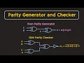
Hey, friends welcome to the YouTube channel ALL ABOUT ELECTRONICS. So in this video, we will see the circuit for the parity generator, and the parity checker. Now in the one of the earlier videos, we already learned about the parity.
So this parity bit, is the additional bit which is used with the data bits for the error detection. And we have also seen that, there are two types of parity. That is odd parity, and the even parity.
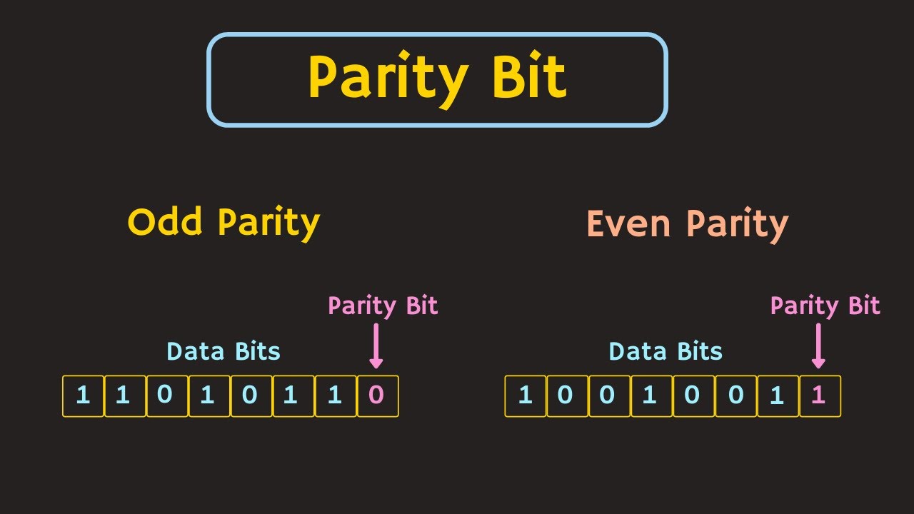
So in case of the odd parity, the total number of 1's in the code, including the parity bit should be equal to odd. For example, let's say we have a seven data bits, and as you can see in this case, the total number of 1's in the data bits is equal to four. Therefore for the odd parity, this parity bit should be equal to 1.
Likewise if the total number of 1's in the data bits is equal to odd, then for the odd parity, this parity bit will be equal to zero. That means based on the total number of 1's in the data bits, this parity bit is set. Similarly in case of the even parity, the total number of 1's in the code, including this parity bit should be equal to even.
So for example, in the data bits, if the total number of 1's are even, then for the even parity, this parity bit will be set as one. On the other end, if the total number of 1's in the data bits is equal to even, then this parity bit will be set as zero. So in this way, by calculating total number of 1's in the data bits, this parity bit is set.
So the question is, how to design this parity generator circuit. So here, we will understand it, with the help of 3 bit parity generator. And first, let us take the example of the even parity generator.
So let's say, we have a three data bits A B and C, and the output parity is equal to P. So based on the data bits, this parity bit will be generated. That means if the total number of 1's are even, then this parity bit will be equal to zero.
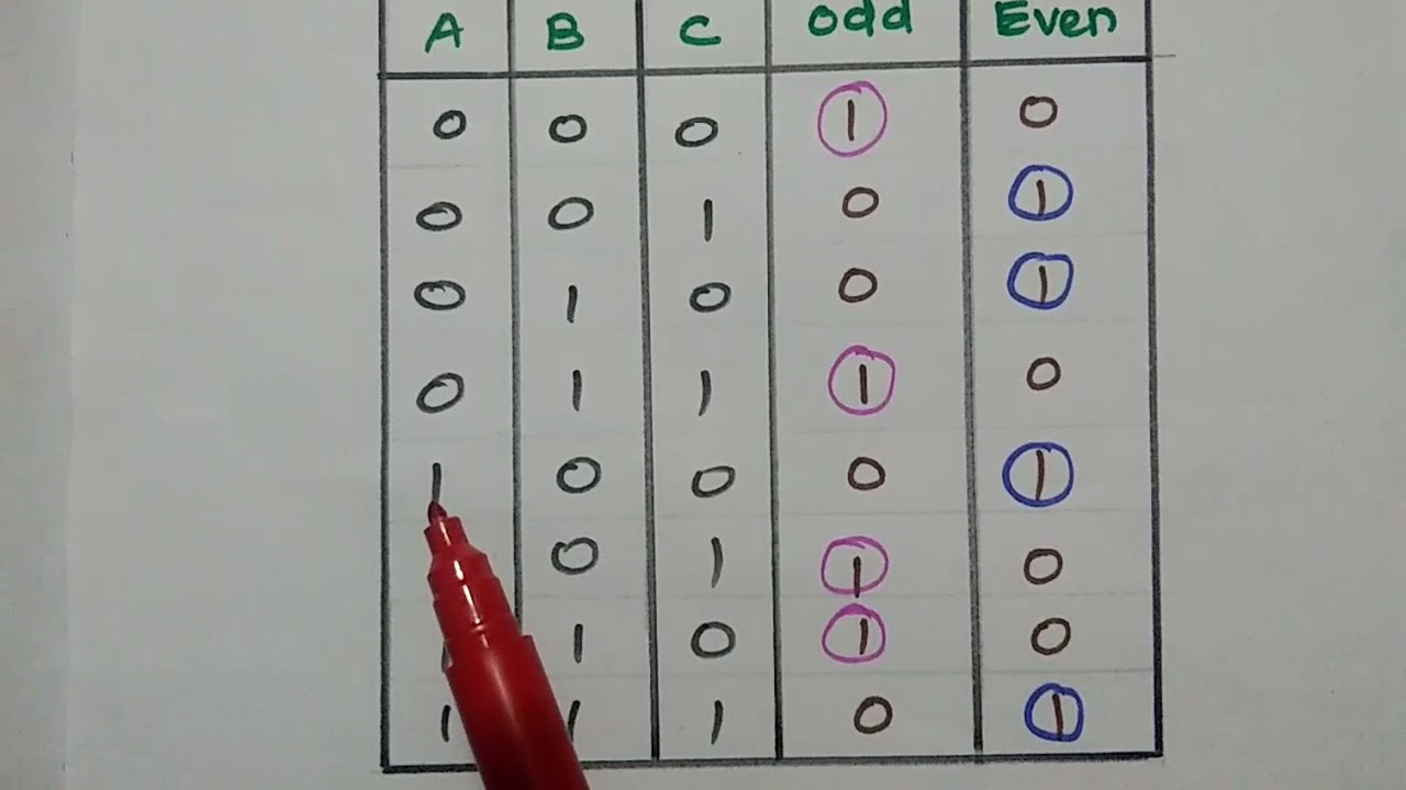
On the other end, if the total number of 1's in the data bits is equal to odd, then this parity bit P will be set as one. So to design the circuit, first of all let us see the truth table of this parity generator. So for the three bits, we have total eight different combinations.
right? And the output P will be equal to one, when the total number of 1's in the data bits is equal to odd. So as you can see, for the four different combinations, this output P will be equal to 1.
And in all four cases, the total number of 1's in the data bits, is equal to odd. So with the help of this truth table, we can easily find the Boolean expression for this even parity generator. So as you can see, for the four different input combinations, this output P is equal to 1.
So algebraically, this is the expression of the P. So here the output P, is written in terms of the sum of minterms. Now in this expression if you see, then from the first two terms, this A bar is common, while from the last two terms, this A is common.
So now in the bracket if you see, there in one bracket, we have B bar dot C, plus B dot C bar. And that is equal to B ⊕ C. On the other end, in the last bracket if you see, then we will have this B bar dot C bar, plus B dot C.
And that is equal to B (XNOR) C. Or in other words we can say that, that is equal to B ⊕ C whole bar. So here let's say this B (XOR) C is equal to X.
That means this expression, can be written as A bar dot X plus, A dot X bar. And that is equal to A (XOR) X. And here we have assumed that, this X is equal to B (XOR) C.
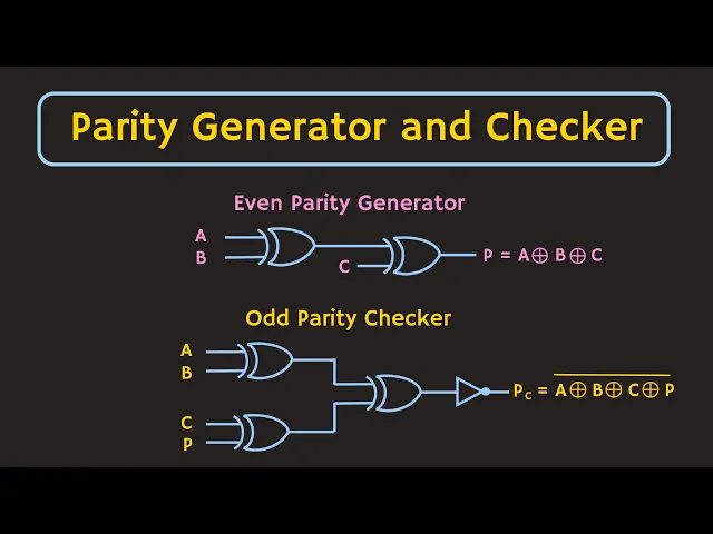
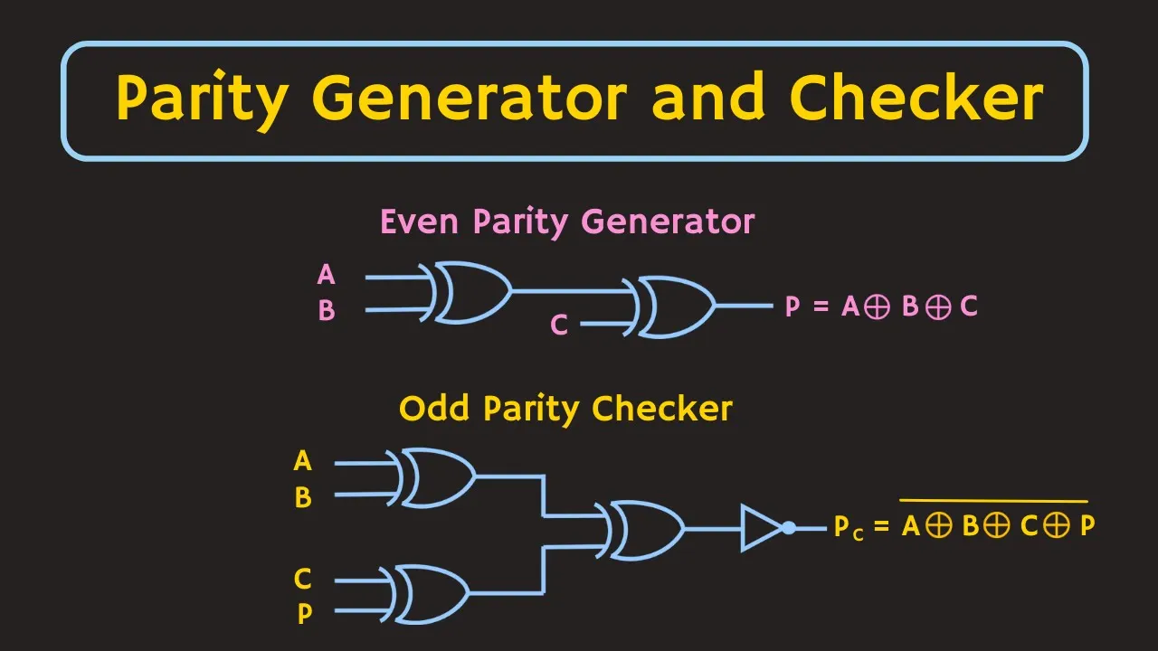
That means, the overall expression of this parity generator, is equal to A ⊕ B ⊕ C That means we can implement this even parity generator, with the help of the XOR gates. And this is the logic circuit of the even parity generator. So similarly, now let's see the logic circuit for this three bit odd parity generator.
So in this odd parity generator, the output P will be equal to 1, when the total number of 1's, in the data bits is equal to even. And the output P will be equal to 0, when the total number of 1's in the data bits is equal to odd. So once again, to find the logic circuit, first of all let us see the truth table of this parity generator.
And here, for the three different input combinations, we have total eight different possibilities. So in this case, this P output is equal to 1, when the total number of 1's in the data bits, is equal to even. So if you see the truth table of this odd parity generator, then this output P column, is the exact complement of the event parity generator.
Because in the even parity generator, the output P was high, when the total number of 1's in the data bit was odd. On the other end, in this odd parity generator, the output P is equal to 1, when the total number of 1's in the data bits is equal to even. So in this odd parity generator, since the output P is the complement of the event parity generator, so we can say that this P is equal to A ⊕ B ⊕ C whole bar.
That means to implement this three bit odd parity generator, we just need to add the NOT gate, in front of the even parity circuit. So this is the logic circuit of the 3 bit odd parity generator. So in this way, with the help of the XOR gates, we can design the even and the odd parity generators.
So similarly, now let's see the logic circuit for the parity checker. So this parity checker circuit, will check the parity of the received code, and it will decide, whether the received code is correct or not. So let us understand the working of this parity checker, with the help of few examples.
So let's say, on the transmitter side, we are using the odd parity. So for the given data bits, for the odd parity, this parity bit P will be equal to 1. Now let's say, including this parity bit, this overall code, is transmitted from the transmitter side.
But at the receiver end, due to noise let's say one of the bits get flipped. Now at the receiver, the parity checker circuit will check the parity of the received code. And in this case it will find that, the overall parity of the received code is equal to even.
But since we are using the odd parity, so it will generate the error. Similarly in case of the even parity, if there is an error in the received code, then this parity checker circuit will generate the error. So let's say the given code is transmitted from the transmitter side.
But due to the external noise, the one bit gets flipped at the receiver end. So when the parity checker circuit, will check the parity of the received code, then it will find that, the overall parity of the given code, is equal to odd. And since we are using the even parity, so it will generate the error.
So in this way, by using the parity checker circuit, we can decide, whether the received code is correct or not. But the thing is, this parity checker circuit will generate the error, when the total number of errors in the received code is equal to odd. So if the total number of errors in the received code is even, in that case this parity checker circuit will not be able to detect the error.
For example in the same case, suppose we have a two number of errors, then as per this parity checker circuit, the overall parity of the received code is equal to even. And since we are using the even parity, so it will not generate any error. That means this parity checker circuit, will not be able to detect the error, when the total number of errors in the received code is equal to even.
But it can detect any odd number of errors in the received code. For example, if the total number of errors in the received code is equal to 3, then in that case, this parity checker circuit will be able to detect the error. Because in this case, once the parity checker circuit checks the parity, of the received code, then it will come out as odd.
And since we are using the even parity, so it will generate the error. That means this parity checker circuit, can detect the odd number of errors. And the same is also true, even for the odd parity.
That means suppose at the transmitter side, if we are using the odd parity, and at the receiver, if we have a two number of errors, then the parity checker circuit, will not be able to detect that error. But on the other end, suppose we have a three number of errors, then the parity checker circuit, will be able to detect that error. That means irrespective of, whether we are using the odd or the even parity, the parity checker circuit can detect the odd number of errors.
Alright, so now let's see the logic circuit, for this parity checker. And first let us start with the even parity checker. So the logic circuit for this even parity checker, is very similar to the parity generator.
But in this case, we will have one more input. And to understand the working, here let's take the case of four bits. So let's see, we have a three data bits, and one parity bit.
And since we are using the even parity, so this parity bit P, is set as 0. Now including this parity bit, this overall code is sent to the receiver. But due to some external noise, one of the bit gets flipped.
Let's say this C bit gets flipped. So now once the parity checker circuit, checks the parity of this overall code, then it will find that, there is an error in the received code. Because now the overall parity of the received code, will become odd.
So in this case, it will generate the error. That means, in such case, the output of the parity checker circuit will become 1. That means, whenever there is an error, then the output of the parity checker circuit will become 1.
And whenever there is no error, then the output of the parity checker circuit will become 0. So to design the circuit, first of all let us see, the truth table of this even parity checker. And in this case as you can see, for the 4-bit received code, we have total 16 different input combinations.
So the output of this parity checker circuit will be high. Or in other words, it will generate the error, when the total number of 1's in the received code is equal to odd. So in this case as you can see, it will generate the error for the 8 different input combinations.
So earlier we have seen that, to find the odd number of 1's we can use the XOR function. So similarly in this case, the output of the parity checker circuit can be defined with the help of XOR function. That means this Pc is equal to A ⊕ B ⊕ C ⊕ P.
So of course, one can also find the same expression with the help of K-map. But earlier we have already seen that, this XOR function can be used for finding the odd number of 1's. And therefore here I am directly writing the expression.
So this expression can be easily implemented with the help of XOR gates. So this is the logic circuit for the 4 bit even parity checker. So similarly now let's see the logic circuit for the odd parity checker.
And once again let us take the case of 4 bit. So let's say, we have a 3 data bits, and 1 parity bit. And for the odd parity, this parity bit P is set as 1.
Now at the receiver, due to the external noise, let's say the 1 bit, gets flipped. And this bit C becomes 0. So now once the parity checker circuit will check the parity, then it will find the error.
And in case of the error, the output of the parity checker circuit should become 1. So once again to find the logic circuit, let's draw the truth table for this odd parity checker. And here for the 4 bit received code, we have total 16 different input combinations.
So in this case, the output of this parity checker circuit will be high, when the total number of 1's in the received code is equal to even. Or in other words it will generate the error, when the total number of 1's in the received code is equal to even. So if you compare the truth table of this odd parity checker, with the even parity checker, then this output column is exactly the complement of the even parity checker.
And therefore we can write that, this parity check Pc is the complement of the even parity checker. That means this parity check is the complement of this A ⊕ B ⊕ C ⊕ P. So if we want to implement this odd parity checker, then we just need to add the NOT gate in front of the even parity checker.
So in this way, with the help of the XOR gates, we can easily design the parity generator as well as the parity checker circuits. And if required, one can also use the readily available IC for this parity generation, as well as the parity checking. So this 74180 is one such IC, which can be used for the parity generation, as well as the parity checking.
But I hope in this video, you understood how to design this parity generator and the parity checker circuits. So if you have any question or suggestion, then do let me know here in the comment section below. If you like this video, hit the like button, and subscribe the channel for more such videos.