Hi, we are at module 40 now. In this module, I am going to design the datapath elements in verilog. So, for the GCD problem, in the last module, I left off at a point, where the gray-box description of the data path inside the GCD module was ready.
And in this module, I am going to show you how to write the various datapath elements. And in this video, we will finish the data path description of the complete design. So, let us switch to the verilog description.
So, one of the things that I did not do earlier is I wrote all of this. How do I know the syntax is correct or not. So, I did not check it earlier.
So, the first thing I am going to do is take the description that I had for the GCD machine itself This is the GCD machine. And I am going to just run. So, I do not have a test bench right now.
So, you can see that, there is no test bench; it is an empty test bench. And I just clicked run. And when I clicked run, I got several errors.
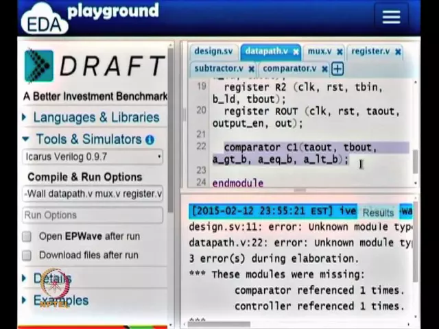
Let us see what the errors are. The first error says unknown module type controller; the second error says unknown module type data path. Of course, that is suppose that is expected, because I said controller C1 datapath D1.
And I did not give any description for datapath or the controller yet. And it said these modules were missing. Now, let me go and look at the file called datapath dot v.
This is actually giving the description for the datapath. And the datapath has several things like subtractors, mux, register, and comparator. So, one thing I can do on the EDA platform is I can say go and use datapath v also.
So, compile data path v also when you compile the design dot sv file. So, if I save that and run it, at least the datapath complain should not happen. So, let us go and look at what complaints we got this time.
So, it says there is still an unknown module type called controller. We have not written the controller; but now, the complier looked at the datapath. In the datapath, we had two subtractors, two muxes, three registers and a comparator.
And we have not designed those so far. So, instead of writing all the verilog and then compiling in one go, I am writing small pieces of verilog; I will get it compiled, so that if there are any syntax errors, I will fix them right away. So, the only errors that I have are the references.
So, I do not know what. So, let us see what are these things. The comparator is referenced ones; controller is referenced ones; mux is referenced twice; register is referenced thrice; subtractor is referenced twice.
And these are not descriptions that I have given yet. But, that is ok, there is no harm in this. So, I am now going to write the design descriptions for multiplexer and what not.
So, let us look at the datapath once more. So, the first thing I need is… So, let us start with the multiplexer because it is the easiest. So, I will cut and paste the design description that I need.
Remember for the multiplexer, I said it is the output, select line, the 0 pin and the 1 pin So, these are the four things that I need. So, I am going to design something called mux dot v. In mux dot v; so the module name is supposed to be mux.
So, I have cut it… I did cut and paste, so that I know exact order in which I am supposed to give things. So, this is supposed to be… The first one is supposed to be the output; I can just call it out now. The next line is supposed to be the select line; I will call that sel.
Then, the input on pin 0 and the input on pin 1. So, this is… These names in0 and in1 are local to the multiplexers descriptions; that is it. We have done this before.
in0, in1 select, and output – these are the four ports that the multiplexer has. So, let us do the descriptions for the port. So, output… So, out is actually a 7 to 0 output.
So, the reason why… So, output – remember – this is supposed to take the same bit as the datapath elements. So, again if you go and look at the picture; this picture here says this is an 8-bit line and this is an 8 bit line. So, this multiplexer is going to select either this 8-bit line or this 8-bit line and present it as the output; which means the design description for the subtractor, the multiplexer, the register – all of them will have 8-bit values.
So, I am going to do that right now. So, the multiplexer has an output, which is an 8-bit value. There are two inputs in0 and in1; which are again 8-bit values.
And there is a single-bit line called select, which is supposed to select either in0 or in1 So, this takes care of the wiring connections. So, now, we need to write the design description for it. I am going to use the familiar always block; always act select or in1 or in2.
So, what this is going to do is if either the select changes or input1 changes or input2 changes; I am This is the combinational circuit; output is supposed to change. So, this is what we needed. So, the interesting thing is that, in1 and in2 are now 8-bit values.
So, in1 is an 8-bit value and in2 is an 8-bit value. And if any of the bits in input 1 changes or if any of the bits in input 2 changes – it is supposed to be in0 and in1. So, any of the input bits in in0 or in1 – if they change; I want the multiplexers output to reflect that.
So, instead of specifying each and every bit as in0 of 7 or in0 of 6 or in0 of 5 and so on; if you just give the whole vector; the always block will get triggered if any of the bits in the vector changes. So, if in0’s bit – even if one of them change; then the multiplexer will react to that; and the output of that will change. So, that is the sensitivity list.
So, in the sensitivity list, if I have a vector, I can specify the whole vector if in this case, multiplexer is supposed to pick the whole thing. So, I specify the whole vector. So, let us go and write the design description.
So, if select equals 0; then we want output to follow in 0; else, we want output to follow in1; it is as simple as that. So, that is all we need. We need output, select, in0, in1.
So, this is I have put it in a file called mux dot v; let me save it. Let me go back to the design file now and run it. Now, at least I should get one less error.
Let us see the errors that are coming up. So, I did not include mux dot v. So, let me include mux dot v.
I will save this. And if I run it; so you can see that, this error that I had earlier – that multiplexer is referenced two times; that error is not coming any more. So, we have a comparator, controller, register, subtractor; we know that, these are not defined yet But, the error on multiplexer is gone.
Also, thankfully, I did not make any mistake in multiplexer either. So, there is no mistake that is coming up here. If I made a syntax error in multiplexer or something else; then the error will come up here also.
So, we do not have that now. Let us move to the next design. So, I am going to call that register.
So, register is the next thing that we needed. Again, if we go and look at the datapath; let us see what the register is supposed to have Register is supposed to take clock reset, input, load enable and output. Again, as before, let me just start with the cut and paste, so that I will have the design description ready, the interface description ready.
So, I want a module called a register, which is supposed to take clock reset. I am just going to call these other lines with local names, which are different. So, I am going to have output, load enable and input.
So, these are the different things that I need. Again, I need to go and specify whether these are inputs and outputs and what not. So, clock and reset are inputs; then we have in itself as an 8-bit value.
Load enable is again an input, but that is a single-bit input; and out is an 8-bit value. So, I will start with that. So, this is fairly straightforward.
We have that. And once we are done; so what we need is we need to specify a bunch of things. So, what do we need?
We need to specify that, the register on either reset or on load – it is supposed to do different things. And we decided that, the whole thing will be a synchronous circuit. So, there is nothing which is going to be asynchronous.
So, what I will do is I will take always add posedge of clock; always add posedge of clock. So, at this point, I already know that, the clock is triggered; which means at this point, if I sample reset; if reset is 1; I want the output to be 0. So, this is always a safe thing to have.
If reset is 1, output is 0; else, if load is 1 or load enable I called lden; if load enable is 1; then output is supposed to follow the input. So, let me reduce this; output is supposed to be the input itself; which I call in. And if you do not put an else clause here, it is okay; because if you do not have an else clause, it means remember the old value, which is given.
So, the old value is whatever the output was – it will just remember it. So, this is just a register, which takes a parallel load – as parallel input as a… So, it has an 8-bit input, which it will take as a parallel input; and it is going to give it out as a parallel output. The only thing is if reset is 1, the output is initialized to 0; else, if load enable is 1 So, there is a priority in order in which things are checked.
If reset is on, it will override everything else; otherwise, if load enable is on, the output will follow the input and this is the end of this module description. So, it is as simple as that. So, it is not very hard.
If you see that, the way in which I am taking things is very organic; it is taking like one small step at a time without you having to worry about everything. Once you have the hardware picture with you; I am writing verilog in small chunks. So, I can now go and add register dot v in the design file.
So, I am including that in the compile options. And I am going to run it. So, again this run is only an empty run, because I do not have a test bench or anything.
So, all I have is just the design descriptions. I am just ensuring that, there are no syntactical errors. So, again I notice that, the registers reference is gone.
So, the register is… And it also looks like register had no errors. So, so far we are good. Now, let us go and write the subtractor and the comparator.
So, again let us go and look at what a subtractor is supposed to take. The subtractor I am expecting that, there are two inputs and there is an output. So, even though it is called taout, tbout and t1; again if we go and look at the picture; taout is actually an input to the subtractor and tbout is actually an input to the subtractor.
So, they are called aout and bout because they are coming out of the registers. So, there are two inputs followed by the output in the subtractor. So, let me copy that.
So, module subtractor. So, I am going to call this input 1, input 2, output – simpler names. So, I do not need to carry the names from the external world.
I will just give internal names which make sense. So, there are… This is a combinational circuit. And in this combinational circuit, if it supposed to take the input on the first pin and take the input on the second pin and subtract one from the other; that is all it needs.
So, what I am going to do is I will declare them whether these are inputs and outputs and what not. So, in1 and in2 are both inputs; I will declare them as such; and out is an output. And since this is a combinational circuit, I am going to write it as always at in1 or in2 If either one changes, the output is supposed to change.
And now, I am going to show you something, which is slightly different. So, I am going to write out as in1 minus in2. This is something that I have not introduced to you so far.
So, what I did now is… So, I can go and write a subtractor. So, I can go and do a design description for a subtractor, which is very very careful; I pick the basic gates and what not. But, verilog also has what is called a behavioral description.
So, in this case, the behavior that we want is in1 minus in2. So, this minus stands for subtraction; verilog allows you to do that. Even though in your home work that I have explicitly said go and design an adder, which will go and instantiate half adder and full adder and so on; technically, if you did out equal to a plus b; so that is acceptable in verilog.
So, here in1 minus in2 – it is supposed to be a subtractor. And tools can actually infer this and say that, this is a subtractor; if there is a subtractor description available, it can instantiate a subtractor directly. So, this is something that tools can do.
So, from verilog, when it looks at minus, it will just interpret this as subtract one from the other. And I am going to leave it at that. So, I have not done a design of subtractor, which uses the basic gates.
So, I have taken it at a slightly higher level for a programmer, who is comfortable. This is probably better because verilog can actually pick the appropriate set of gates and optimize it and so on. So, you can give it to what is called a synthesis tool.
A synthesis tool when it sees in1 minus in2, it will go and pick an appropriate subtractor based on the constraints that is given. So, this is not something that we have talked about so far. But, I have kept it at a level of abstraction, which is high rather than instantiating basic gates and so on to get a subtractor.
So, let me now save this. And as before, I will add subtractor dot v to the design. I will save it and run it.
So, just to ensure that, there are mistakes in the subtractor. So, it is always a good idea to ensure that, anything that you write; it is actually syntactically correct, because otherwise, too many errors will accumulate and so on. So, again the subtractor’s warning is gone and there is an error on the subtractor right now and it looks like the subtractor itself is having no error.
So, somehow magically, when I am typing code, it looks like there is no error that I am making at all. But, this comes with years of practice and experience. So, you may make mistakes when you design things and it is better to actually go and check each one of them out to ensure that, there are no syntactical or semantic errors.
So, in this case, I know that, input 1 and input 2 – both of them should be on the sensitivity list; and minus will work and there is a semicolon needed. So, I know all of this from years of verilog design. So, I have put all of that right now.
So, the final beast that I am going to decide or design is the comparator. So, let us go and look at what the comparator is supposed to do. The comparator is supposed to take two inputs and it is supposed to give three individual bits as output.
So, let me copy the design description. So, comparator – module comparator is supposed to take several inputs. So, let we call them a and b here, because it is supposed to be comparing a and b.
So, it compares two numbers: a and b and gives three bits: a greater than b, a equal to b, and a less than b as output. So, let me put the design description. So, a and b are 8-bit values and they are inputs.
a greater than b, a equal to b and a less than b are all outputs and they are single-bit outputs So, this takes care of the design interface description. So, now, I have to go and write the comparator itself. So, again I am going to use the always block for this either in one… So, either a changes or b changes; if either one of them changes, then the comparator is supposed to change the output.
So, here what I am going to do is I am going to do a series of comparisons. Again, I am going to introduce something new in verilog that you have not seen so far. So, I am going to check if a greater than b.
This is just like what you do in programming languages. So, instead of comparing them bitwise, I am letting verilog use the comparator operator. So, that is comparator operator a greater than means a and b are interpreted as… So, these are 8-bit values.
The 8-bit interpretations of a and b are used directly. And so there are two things: when the complier in the simulator runs, this is greater than as a simple operation. You take the 8-bit value and compare with the 8-bit value; but later, when we want to infer a circuit for this, the synthesizer will go and look at a greater than b and generate an appropriate circuit for this.
So, if a is greater than b, then we know that, we want these three names. So, again I am going to show you something new here. So, I want these three values.
I need only one of them to be on. So, I know that, this a greater than b should be on; a equal to b, a less than b – these two should be off. So, one way to do that is I am going to put something here, which is new to you again.
So, on the right side, what it says is I am giving a 3-bit vector and they are all in binaries. This three means I am giving you three bits. So, I am giving you three values.
This 1 0 0 is three values. And these three values; what they mean is they are interpreted as bits. So, let us look at the left side versus right side.
So, if a is greater than b, I want a underscore greater than underscore b to be on. So, these three values on the left side will take the corresponding values on the right side So, a greater than b will take 1; a equal to b will take 0; a less than b will take 0 So, that is what this statement is supposed to be. On the left side, we have grouped three bits together by putting what is called the set bracket; on the right side, I have what is called a bit vector.
The bit vector is a 3-bit vector. So, this b says it is a bit and this 3 says it is a vector; and the values that is supposed to be in the vector are 1 0 0. So, that is the first line.
So, if a greater than b; then it is this; then I am going to do else if. So, I can now check if a is equal to b. If a is equal to b, then we have again the same thing I am going to cut and copy.
Now, instead of 1 0 0, the vector is 0 1 0. Finally, if this is also not true; then it has to be the case that, a is less than b. So, in which case, I will put 0 0 1.
So, let us see what we have done here. So, maybe I will reduce the font size, so that you can see what it is. So, let us see this.
Always add a or b; if a is greater than b, then these three single-bit values will take 1 0 1 0 correspondingly. If else if a is equal to b, then these three bits will take the corresponding value 0 1 o And otherwise, they will take 0 0 1. And… So, I am going to use the less than symbol here.
So, I am going to use this statement, which is a signal-assignment statement. So, I will talk about this later and we are done. So, this takes care of the comparator also.
So, if a or b changes; then this always block is evaluated and you will get one of these output bits to be a 1. So, let me again save this. And I am going to add comparator also as a file.
Go back to design, save it and run. So, hopefully, the controller… Nice; so the only thing that is missing. So, we have compiled all of these and it says the unknown module type controller.
It looks like the comparator itself again has no mistakes. So, what we have done is the datapath was instantiating 2 subtractors, 2 multiplexers, 3 registers and a comparator. For each one of them, we have given the design descriptions.
So, there are four design files, which takes care of each one of them. The only thing that is left out is the controller itself. And the controller… So, we have the state machine what we will do in the next module is will take the state machine and I will show you how to write the state machine as a verilog code.
So, so far, we have done quite well. So, we have started from a vague algorithmic description of the problem, which is the Euclid’s algorithm. That algorithm itself maybe new to you; but if the algorithm is given to you, from there we identified what are all the different components that are needed.
We took all of the components and we did a hardware diagram. The sequencing of the hardware is still something that we have not figured out. We need the state machine, which we did as a picture; we need to go and write the for verilog for it And we have done a top-down design of verilog.
Starting from the design description, we put the controller in the datapath. For the datapath, we need the subtractor, the multiplexer, the register and the comparator; we have designed all of that. The datapath design is complete now; that is it.
The datapath design is over. The only thing we need is we need to put the controller – the state machine for the controller; once we write the verilog code for that, the overall description is done. Then, we can write a test bench and test it and ensure that the whole thing is working fine So, it may seem to you that, this thing is magic and all of these are working nicely and so on is just that, I have taken a lot of care in drawing the diagram, taking the diagram and putting it into the verilog ensuring that, all the connections are in the proper order And verilog syntax itself did not come in my way.
If you are a new programmer in verilog, all of these could be daunting. They are not going to be simple task that you can do in a short period of time. You will take a lot more time to do it, but that is okay.
So, you have seen me. Now, what I will put all these files in the folder later. You can take these and play around and see how each of these descriptions are provided to you And you will also be able come up with these things once you practice.
So, one thing with programming languages is that, you have to keep practicing with more and more design problems; only then the languages syntax and various semantics and so on stick with you. So, if you learn and then if you forget for sometime; if you do not practice; after one month or so you will not remember anything at all; you have to keep practicing programming languages specifically, so that you remember it well. So, this is just like playing a musical instrument or things like that; where unless you practice continuously, you may get out of touch.
So, this brings me to the end of this module. In the next module, we will see how to design the state machine. And finally, we will put the state machines, the controller and the datapath together and we will write a test bench.
The test bench will test the GCD machine. So, thank you and I will see you in the next video.