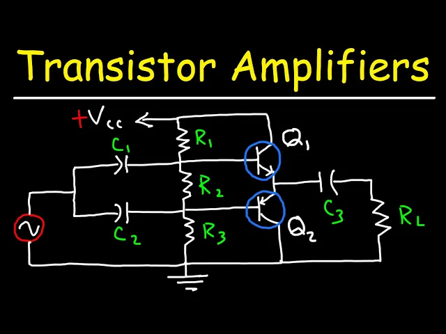
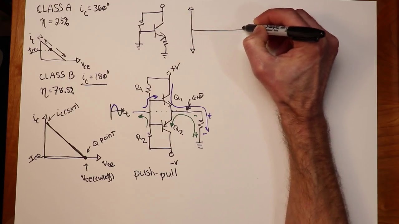
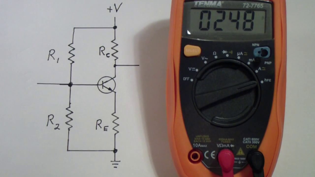
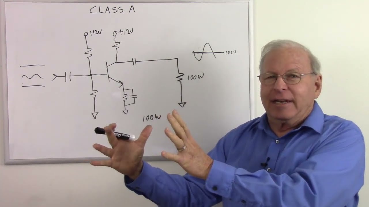
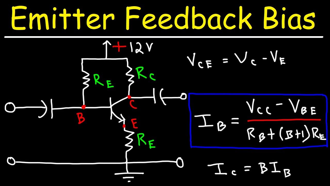
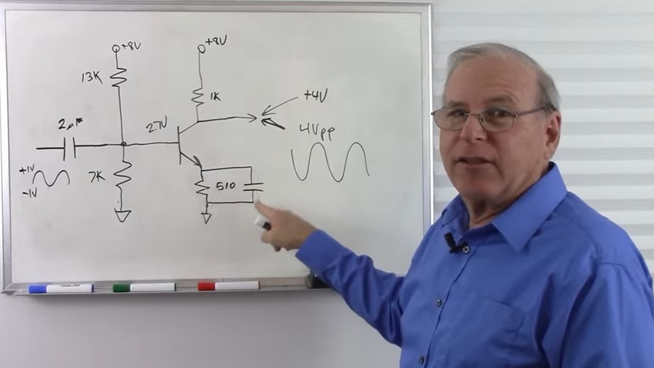
in this video we're going to talk about the different types of transistor amplifiers such as the class a amplifier the class a b amplifier the class b amplifier and the class c amplifier there's also the class d amplifier but we're not going to touch that one in this video so let's draw the circuit for the class a amplifier we're going to start with an npn transistor this is the base of the transistor that's the collector and this is the emitter we're going to connect the emitter to a resistor which we'll call re the emitter resistor rb is the base resistor and then rc the resistor associated with the collector now rc and rb they will be connected to vcc the collector supply voltage which would be the positive terminal of the battery and then typically there's another resistor which we'll call r1 rb and r1 they form a voltage divider now the capacitors c1 and c2 are coupling capacitors they're used to block dc but they will pass an ac signal and then we have the ground and then typically you'll find connected across the emitter resistor is a bypass capacitor it allows the ac signal to bypass the emitter resistor thus increasing the voltage gain of this circuit so here we have an input signal and then at the output we're going to have an inverted but larger output signal and so the function of an amplifier is to increase the power level of an ac input by transferring power from the dc power supply to the input signal the voltage gain of the amplifier is the ratio of the output voltage to the input voltage the efficiency of the amplifier is the ratio of the ac load power divided by the power delivered by the dc power source times 100 so this is the class a amplifier also known as the common emitter amplifier it has a maximum efficiency that is a maximum theoretical efficiency of 25 percent the actual efficiency will usually be less than that but that's the maximum theoretical efficiency and so as you can see this amplifier is not very good in terms of or being used as a power amplifier it's more appropriately used as a small signal amplifier because its efficiency is so low now this particular transistor conducts for the entire 360 degrees of the input cycle so q1 which is this transistor that's a terrible circle is always on in this case one advantage of the class a amplifier is that it has very little to no distortion which is good even though the efficiency is very low now in order to design a circuit with an efficiency that is close to 25 as possible you want to set vce that is the voltage between the collector and the emitter pins of the transistor to one half of the collector supply voltage so if the collector's supply voltage is 9 volts you want to design a circuit in such a way that vce is as close to 4. 5 as possible now keep in mind vbe the voltage between the base and the emitter is going to be between 0. 6 and 0.
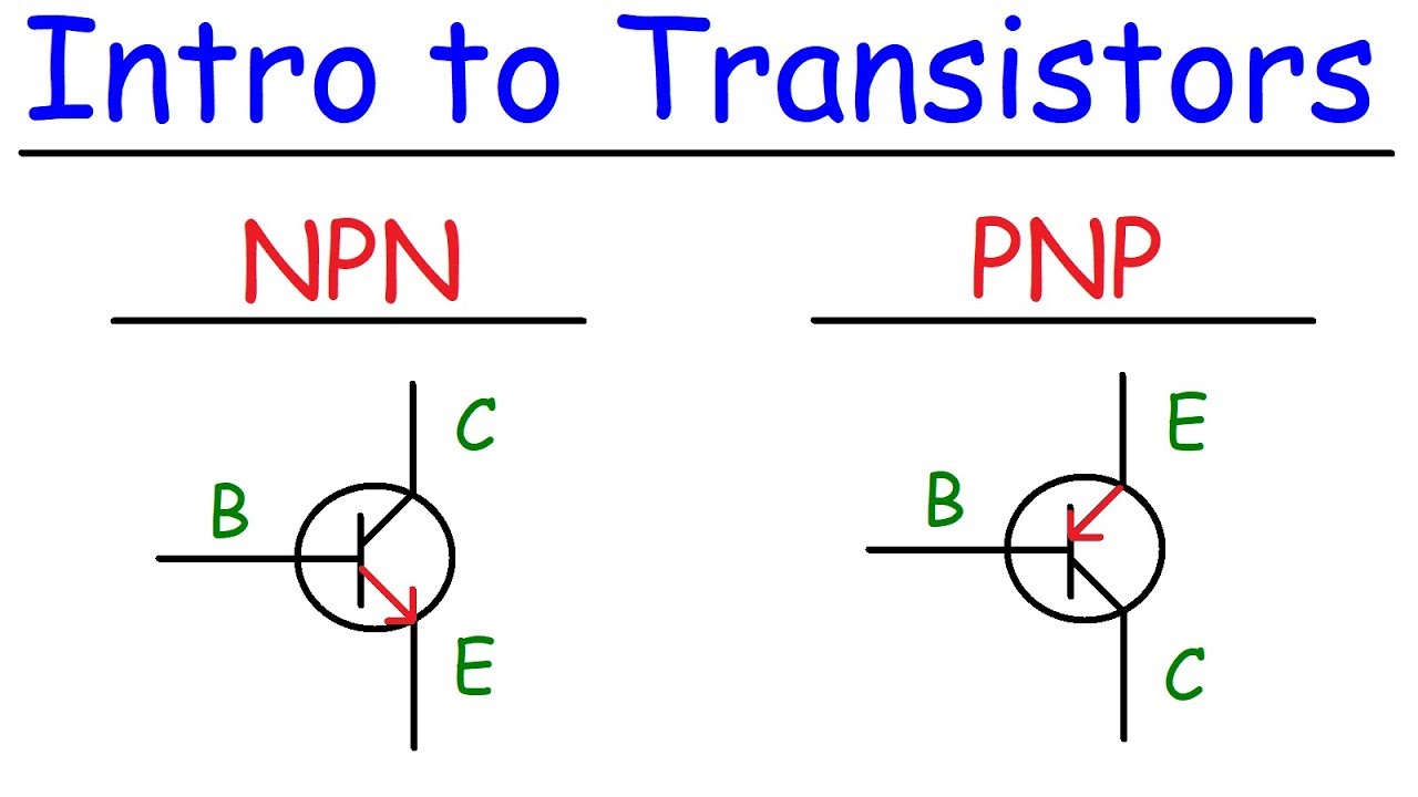
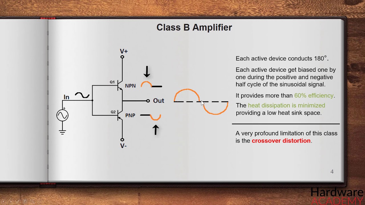
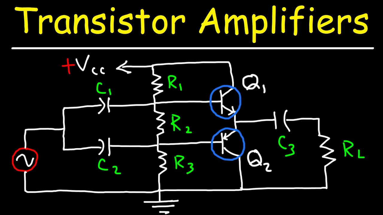
7 volts and ic is equal to beta times ib where beta is equal to hfe beta is the ratio of the collector current to the base current so those are some things that you want to know when dealing with the class a amplifier or the common emitter amplifier now there's something that you could do to increase the efficiency of the class a amplifier and in order to do that you need to replace rc with another element that is a transformer and so what we have here is a transformer coupled class a power amplifier so the output is going to be across the secondary part of the transformer what you could do is replace it with a load resistor if you want to and so with this particular transformer coupled class a amplifier the theoretical efficiency is no longer 25 but the maximum theoretical efficiency is 50 percent now to actually achieve this is not easy in actuality your actual efficiency might be less than 40 you might be getting efficiencies of 35 39 or something like that but the maximum theoretical efficiency is 50 now here's a question for you why is it that replacing rc with a transformer increases the efficiency of the circuit why is that it has to do with the fact that the transformer like an inductor can absorb and release stored energy using its magnetic fields let's set the collector supply voltage to 12 volts now keep in mind the input current is fluctuating so the base current is fluctuating and thus the collector current is fluctuating as well as the collector current increases the magnetic field that is generated by the transformer that field is going to increase in strength and so during this process energy is being stored by the transformer and so there's going to be an induced emf generated by this transformer at this point the transform is absorbed in energy and just to keep things simple let's say that the potential across the transformer is eight volts so these two voltages they go against each other so at point c the voltage will be four volts with respect to ground now the current won't increase forever eventually the current is going to come back down when the current decreases the magnetic field collapses and that stored energy is released back to the circuit the polarity across the transformer reverses and so this is now positive and the other side is negative and let's use the same value just to keep it simple 8 volts so now the potential at point c will be the sum of 8 and 12 volts so it's going to be 20 volts so notice that the potential is higher than the collector supply voltage and as a result this increases the efficiency of the transformer coupled class a amplifier circuit now the next type of amplifier that we're going to talk about is the class b amplifier the class b amplifier it uses two complementary transistors an npn transistor and a pnp transistor let's call this q1 and q2 so q1 is an npn transistor you can easily distinguish it from a pnp transistor due to the fact that the arrow points away from the center of the transistor in the pnp transistor the arrow points towards the center now we need three resistors one of which will be between the bases of the two transistors so we're going to call this r1 r2 and r3 now the input signal is going to be coupled through two capacitors and it's going to be connected to the ground as well the output is going to be taken across the load resistor and here is the collector supply voltage vcc so this is the circuit for a class b amplifier the maximum theoretical efficiency for this amplifier is 78. 5 percent now in order for this circuit to work properly the two transistors have to be biased at cut off during the positive half cycle of the input sine wave q1 conducts so q1 is in the on state q2 is off now during the negative half cycle let's put this in blue q1 is going to be off and q2 will be on so for each half cycle only one of the transistors should be conducted if it's designed appropriately the other transistor should be off so each transistor conducts for one half or 180 degrees of the sine wave and so this improves the efficiency of the class b transformer i mean the class b amplifier now there's one problem with this particular circuit besides the efficiency not being 100 and that is crossover distortion the output doesn't look like a nice pure sine wave instead it looks something like this my drawn is not perfect but that's what it is now the crossover distortion is created due to the fact that the emitter base voltage of each of the two transistors is approximately 0. 7 volts so until the input sine wave reaches positive or negative 0.
7 volts the two transistors will be off and so the output voltage will be zero at this point so that's the one disadvantage of the class b amplifier is the presence of crossover distortion now this circuit can be improved by creating what is known as a class a b amplifier and to create the class a b amplifier what you need to do is replace r2 with two diodes and these are silicon diodes with a voltage drop of approximately 0. 7 so to combine the total voltage drop between let's call this point a and point b will be 1. 4 which is equal to the voltage drops of the two transistors which is also 1.
4 now granted the voltage across the silicon diode and the base emitter junction of a transistor both can be between 0. 6 to 0. 7 volts so this could be 1.
2 and that could be 1. 2 but they're relatively close to each other the combined voltage drop will be somewhere between 1. 2 and 1.
4 but that's how you could design the class a b amplifier is by replacing r2 with two silicon diodes and so this will reduce the problem of crossover distortion so that's the advantage of the class a b amplifier now the last amplifier that we're going to talk about today is the class c amplifier this particular amplifier only uses one transistor it's not like the class b or the class a b amplifier that uses two transistors now this amplifier is different from the other ones in that it is a tuned amplifier so it has an inductor and a capacitor in parallel with each other so we'll call this c2 this is c1 and we'll call that l1 and then we have a resistor rb and that is attached to a negative voltage which we'll call negative vbb so that is the class c tuned amplifier the efficiency the maximum theoretical efficiency for this amplifier is pretty high it's 99 however there's a major disadvantage with this amplifier and that is the distortion the distortion can be very severe for this particular amplifier and the second thing is that it conducts for less than 180 degrees of the input cycle so during the positive half cycle that is when it's above 0. 7 volts this side is going to be positive this side will be negative conventional current will flow in this direction charge in c1 activating the npn transistor and when that's activated current will flow from the dc power supply charging c2 and l1 and then oscillations will begin energy will be transferred back and forth between c2 and l1 and so that energy transfer happens during the positive half cycle during the negative half cycle q1 is off if we put a negative sign here and a positive sign here current cannot flow in this direction because the base emitter junction will be reverse bias and so q1 is off during the second half but it's on during the first half when the voltage exceeds 0.