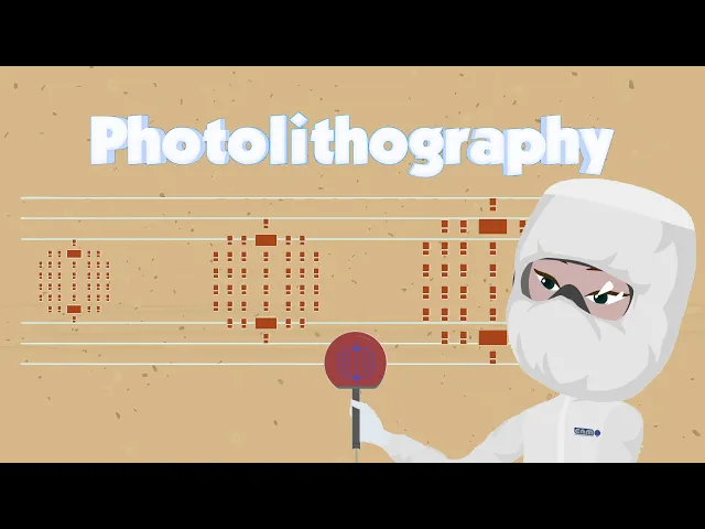
Photolithography is a fundamental process employed in the fabrication of chips or integrated circuits. It involves transferring a pattern from a mask onto the surface of a wafer to create distinct layers of the chip. To achieve this, a photosensitive resist, sensitive to ultraviolet light, is utilized, as we will explore in more detail shortly.
Due to the progressively shrinking size of the transistors constituting the chips, this technique becomes increasingly more delicate, which requires the controlled environment of a clean room. This controlled environment is crucial for preventing the intrusion of unwanted particles, such as dust, which could be larger than certain components of the chip. This is a wafer a thin disc composed of Monocrystalline Silicon, although alternative materials like Silicon Carbide or Gallium Nitride can also be used.
Wafers are typically circular. Various types of photolithography processes exist, each depend on the dimensions of the features to be defined. Here, we will illustrate one of the most common examples.
The first step involves establishing optimal conditions on the wafer surface before applying the photoresist. To do that, we clean the wafer and place it in an oven to bake at a high temperature to dry it. Next, we increase surface adherence by placing the wafer in a unit containing an adhesion promoter.
In this step, the wafer is exposed to steam infused with a liquid chemical compound, creating an ultrathin layer that helps the adhesion of the resist to the surface of the wafer. Now the wafer's ready for the deposition of the photoresist! The next step is a Spin Coating.
We place the wafer into the unit, adjust the parameters and we're ready! The photoresist is deposited onto the wafer's surface. The rotation of the wafer within the unit ensures the even spreading of the photoresist, resulting in the formation of a uniform layer.
Then we place the wafer in the oven again to bake. The wafer must be baked for a few minutes so that the photoresist layer becomes compact. While we wait for the baking process to finish, let’s take a look at the masks, probably the most important aspect of the chip processing.
These are square glass pieces that permit light to pass selectively into specific areas, facilitating the transfer of designed patterns onto the photoresist deposited on the wafer's surface. This crucial step sets the stage for subsequent layer depositions, ion implantation or etching processes, all of which will occur exclusively in the exposed areas. A distinct mask level is used for each photolithography process, and they must be aligned correctly.
The following step is of crucial importance: transferring the pattern design from the mask to the wafer. Since this wafer has no pre-existing exposed pattern, this marks its first exposure in the fabrication process. We will utilize a machine resembling a camera with a flash, known as a mask aligner, to work with the mask.
This crucial part of the process aids in exposing the desired image onto the wafer. This crucial part of the process aids in exposing the desired image onto the wafer. Don’t forget your protective glasses because the flash is ultraviolet light and it can damage our eyes!
It is also possible that the wafer we are processing may not be blank, meaning it may have been processed in previous manufacturing processes. In this case, before exposing another area, the mask must be aligned with the equipment to avoid any overlapping error. We will look through the visor and use the joysticks to carefully overlap the two crosses.
Once that is done, we continue with the exposure. Now we can see the new form taking shape. These steps must be followed carefully to ensure it is well defined.
Whether it's a wafer undergoing its initial exposure or one that has previously undergone processing, the procedure that follows remains the same. Thanks to the baking step, this is no longer a smooth wafer as it already has shapes on the surface. It’s now time for the developing process, which is similar to analogue photography, removing the resist from the areas exposed to ultraviolet light.
First, we take the wafer and submerge it in the basic developing solution. Then it is rinsed in ultra-pure deionised water. Finally, the wafer is dried.
For this we use this ultra-pure nitrogen gun. A few blasts and we’re done. Now we can see big changes on the wafer.
To finish, the resist must be hardened. The wafer must be picked up using vacuum tweezers so as not to contaminate it during handling, this is done for all of the processing steps. And there’s the wafer coated with a hardened resist layer, except for the areas that have been exposed to ultraviolet light!
We’ve just seen a full photolithographic process. Now the wafer with the patterned resist is ready for further ion implantation, layer deposition or etching processes, which will only affect the exposed areas; plus a photolithographic process will be conducted for each level of material. All inside the Clean Room.